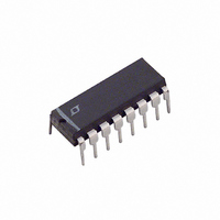
LTC1590CN Linear Technology, LTC1590CN Datasheet - Page 3

LTC1590CN
Manufacturer Part Number
LTC1590CN
Description
IC D/A CONV 12BIT DUAL 16-DIP
Manufacturer
Linear Technology
Datasheet
1.LTC1590ISPBF.pdf
(12 pages)
Specifications of LTC1590CN
Settling Time
1.5µs
Number Of Bits
12
Data Interface
Serial
Number Of Converters
2
Voltage Supply Source
Single Supply
Power Dissipation (max)
55µW
Operating Temperature
0°C ~ 70°C
Mounting Type
Through Hole
Package / Case
16-DIP (0.300", 7.62mm)
Lead Free Status / RoHS Status
Contains lead / RoHS non-compliant
ELECTRICAL CHARACTERISTICS
SYMBOL
Analog Outputs
C
Digital Input
V
V
I
C
Digital Output
V
V
Timing Characteristics
t
t
t
t
t
t
t
t
t
Power Supply
V
I
The
temperature range.
Note 1: 0.5LSB = 0.012% of full scale.
Note 2: Using internal feedback resistor.
Note 3: Guaranteed by design, not subject to test.
Note 4: I
Note 5: OUT1 load = 100 in parallel with 13pF.
Note 6: V
all 1s to all 0s.
Note 7: DAC A output with V
DAC B output with V
loaded with all 1s.
V
IN
1
2
3
4
5
6
7
8
9
CC
OUT
IH
IL
IN
OH
OL
CC
CC
= 4.5V to 5.5V, V
denotes specifications which apply over the full operating
OUT1
REF
PARAMETER
Output Capacitance (Note 3)
Digital Input High Voltage
Digital Input Low Voltage
Digital Input Current
Digital Input Capacitance
Digital Output High Voltage
Digital Output Low Voltage
D
D
CLK High Time
CLK Low Time
CS/LD High Time
LSB CLK to CS/LD
CS/LD Low to CLK High
CLK Low to CS/LD Low
CLK to D
Operating Supply Range
Supply Current
= 0V. DAC register contents changed from all 0s to all 1s or
with DAC register loaded with all 0s.
IN
IN
to CLK Setup Time
to CLK Setup Hold Time
REF B
OUT
REF
Delay
= 0V, V
REF A
= 10V, V
REF A
= 0V and V
= 10kHz 20V
OUT1
REF B
= V
OUT2
= 10kHz 20V
P-P
CONDITIONS
DAC Register Loaded to All 1s
DAC Register Loaded to All 0s
(Note 3) V
I
I
Digital Inputs = 0V or V
OH
OH
. Both DAC registers
= AGND = DGND = 0V, T
= 200 A
= 1.6mA
IN
P-P
= 0V
, or
CC
Note 8: Glitch on DAC A or DAC B output when the other DAC makes a
full-scale transition.
Note 9: 10Hz to 100kHz. Calculation from e
K = Boltzmann constant (J/K ); R = resistance ( ); T = resistor temperature
( K); B = bandwidth (Hz).
Note10: V
LT
Note 11: V
using LT1358 op amp.
Note 12: –3dB bandwidth using LT1358 op amp.
A
®
= T
1124 op amp.
MIN
REF
REF
to T
= 6V
= 10V, 10kHz sine wave, DAC register loaded with all 0s,
MAX
RMS
, unless otherwise noted.
at 1kHz. DAC register loaded with all 1s, using
MIN
2.4
4.5
50
40
40
50
40
20
20
10
4
0
n
0.001
= 4KTRB where:
TYP
60
30
5
LTC1590
MAX
160
0.8
0.4
5.5
90
60
10
8
1
UNITS
3
pF
pF
pF
ns
ns
ns
ns
ns
ns
ns
ns
ns
V
V
A
V
V
V
A


