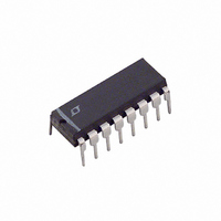
LTC1590CN Linear Technology, LTC1590CN Datasheet - Page 7

LTC1590CN
Manufacturer Part Number
LTC1590CN
Description
IC D/A CONV 12BIT DUAL 16-DIP
Manufacturer
Linear Technology
Datasheet
1.LTC1590ISPBF.pdf
(12 pages)
Specifications of LTC1590CN
Settling Time
1.5µs
Number Of Bits
12
Data Interface
Serial
Number Of Converters
2
Voltage Supply Source
Single Supply
Power Dissipation (max)
55µW
Operating Temperature
0°C ~ 70°C
Mounting Type
Through Hole
Package / Case
16-DIP (0.300", 7.62mm)
Lead Free Status / RoHS Status
Contains lead / RoHS non-compliant
APPLICATIONS
Description
The LTC1590 is a dual 12-bit multiplying DAC that has
serial inputs and current outputs. It uses precision R/2R
resistor ladder technology to provide exceptional linearity
and stability. The device operates from a single 5V supply
and provides a 10V reference input and voltage output
range when used with an external op amp.
Serial I/O
The LTC1590 has a 3-wire SPI/MICROWIRE
serial port that accepts 24-bit serial words. Data is loaded
MSB first with the first 12 bits controlling DAC A and the
second 12 bits controlling DAC B. Data is shifted into the
D
be taken low before transferring data to enable the CLK
input. After transferring data, CS/LD is pulled high to load
data from the shift register to the DAC registers which
updates both DACs.
The buffered output of the 24-bit shift register is available
on the D
one 3-wire interface by connecting the D
pin of the next DAC (see the Timing Diagrams section).
MICROWIRE is a trademark of National Semiconductor Corporation.
TIMING DIAGRAMS
IN
W U
input on the rising edge of CLK. The CS/LD input must
OUT
CS/LD
D
CLK
OUT
D
pin. Multiple DACs can be daisy-chained on
IN
TIMING DIAGRAM
U
t
8
PREVIOUS WORD
INFORMATION
D11 A
U
t
7
W
D11 A
MSB
t
9
W
1
PREVIOUS WORD
OUT
D10 A
TM
pin to the D
t
1
D10 A
compatible
U
t
2
2
PREVIOUS WORD
D9 A
IN
t
4
D9 A
Equivalent Circuit
Figure 1 shows an equivalent analog circuit for the LTC1590
DACs. R is the reference input, R
11k. The DAC output is represented by the Thevinin
equivalent current source with a value of:
The current source I
DAC output switches. I
85 C and decreases by roughly two times for every 10 C
reduction in temperature. C
and it also comes from the DAC output switches and varies
from 30pF at zero scale to 60pF at full scale. R
equivalent output resistance, which varies with digital
input code (see Op Amp Selection section).
V
V
3
t
REF A
REF B
3
(Code/4096)(V
R
D1 B
23
Figure 1. Equivalent Circuit
PREVIOUS WORD
CODE
4096
REF
LKG
D0 B
/R)
V
models the junction leakage of the
REF
LKG
R
D0 B
LSB
OUT
is typically less than 5nA at
24
t
R
6
is the output capacitance,
O
REF
CURRENT WORD
I
, which is nominally
LKG
D11 A
R
t
5
LTC1590
1590 TD02
C
OUT
O
R
R
OUT1 A
OUT1 B
OUT2 A
OUT2 B
AGND
is the
FB A
FB B
1590 F01
7


