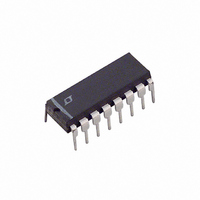
LTC1590CN Linear Technology, LTC1590CN Datasheet - Page 9

LTC1590CN
Manufacturer Part Number
LTC1590CN
Description
IC D/A CONV 12BIT DUAL 16-DIP
Manufacturer
Linear Technology
Datasheet
1.LTC1590ISPBF.pdf
(12 pages)
Specifications of LTC1590CN
Settling Time
1.5µs
Number Of Bits
12
Data Interface
Serial
Number Of Converters
2
Voltage Supply Source
Single Supply
Power Dissipation (max)
55µW
Operating Temperature
0°C ~ 70°C
Mounting Type
Through Hole
Package / Case
16-DIP (0.300", 7.62mm)
Lead Free Status / RoHS Status
Contains lead / RoHS non-compliant
APPLICATIONS
Op Amp Selection
To maintain the excellent accuracy and stability of the
LTC1590 thought should be given to op amp selection.
Fortunately, the sensitivity of INL and DNL to op amp offset
has been significantly reduced compared to competing
parts of this type. The op amp’s V
offset. In addition, because the DAC’s equivalent output
resistance R
code-dependent DAC output error proportional to V
fixed reference applications this causes gain, INL and DNL
error. For multiplying applications, a code-dependent, DC
output voltage error is seen. At zero scale the DAC output
error is equal to the op amp offset, and at full scale the
output error is equal to twice the op amp offset. For
example, a 1mV op amp offset will cause a 0.41LSB zero-
scale error and a 0.82LSB full-scale error with a 10V full-
scale range. The offset caused INL error is approximately
0.4 times the op amp V
amp V
10V full-scale range, the INL degradation will be 0.17LSB
and DNL degradation will be 0.03LSB.
Op amp bias current causes only an offset error equal to
(I
TYPICAL APPLICATIONS
BIAS
)(R
OS
CHIP SELECT/DAC LOAD
. For the same example of 1mV op amp V
FB
)
O
SERIAL CLOCK
changes as a function of code, there is a
(I
DATA OUT
BIAS
DATA IN
CLEAR
U
)(11k ). For example, a 100nA op
OS
INFORMATION
and DNL error is 0.07 times op
U
10
13
14
11
12
15
0.1 F
7
D
CLK
CS/LD
D
CLR
DGND
AGND
IN
OUT
5V
16
OS
U
W
LATCH
24-BIT
SHIFT
REG
AND
causes DAC output
Dual Programmable Attenuator
V
V
V
V
U
10V
10V
IN B
REF B
REF A
IN A
LTC1590
9
1
OS
OS
DAC B
DAC A
. For
and
R
R
FB B
FB A
8
2
amp bias current causes a 1.1mV DAC offset, or 0.45LSB
for a 10V full-scale range. It is important to note that
connecting the op amp noninverting input to ground
through a resistor will not cancel bias current errors and
should never be done! Similarly an offset caused by op
amp bias current should not be adjusted by using the op
amp null pins since this increases offset between DAC
OUT1 and OUT2 pins, causing INL, DNL and gain errors.
If op amp offset error adjustment is required, the op amp
input offset voltage (the voltage difference between OUT1
and OUT2) should be nulled.
Grounding
As with any high precision data converter, clean ground-
ing is important. A low impedance analog ground plane
and star grounding should be used. OUT2 carries the
complementary DAC output current and should be tied to
the star ground with as low a resistance as possible. Other
ground points that must be tied to the star ground point
include the V
input(s) and the V
OUT1 B
OUT2 B
OUT2 A
OUT1 A
3
4
5
6
REF
33pF
33pF
input ground, the op amp noninverting
OUT
2
3
5
6
–
+
+
–
LT1358
LT1358
ground reference point.
1/2
1/2
–15V
15V
8
4
1
7
0.01 F
0.01 F
V
OUT
= –V
1590 TA07
IN
V
V
OUT B
4096
OUT A
LTC1590
D
9


