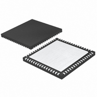
LTC2755CUP-12#TRPBF Linear Technology, LTC2755CUP-12#TRPBF Datasheet - Page 11

LTC2755CUP-12#TRPBF
Manufacturer Part Number
LTC2755CUP-12#TRPBF
Description
IC DAC 12BIT CUR OUT 64-QFN
Manufacturer
Linear Technology
Datasheet
1.LTC2755IUP-12PBF.pdf
(24 pages)
Specifications of LTC2755CUP-12#TRPBF
Settling Time
2µs
Number Of Bits
12
Data Interface
Parallel
Number Of Converters
4
Voltage Supply Source
Single Supply
Operating Temperature
0°C ~ 70°C
Mounting Type
Surface Mount
Package / Case
64-QFN
Lead Free Status / RoHS Status
Lead free / RoHS Compliant
Power Dissipation (max)
-
Available stocks
Company
Part Number
Manufacturer
Quantity
Price
READ (Pin 49): Read Pin. When READ is asserted high,
the data I/O (D0-D15) or span I/O (S0-S2) port outputs the
contents of the selected register (see Table 1). For single-
span operation, readback of the span I/O pins is disabled,
since they must be tied directly to GND and/or V
UPD (Pin 50): Update and Buffer Select Pin. When UPD
is asserted high with READ held low, the contents of the
addressed DAC’s input registers (both data and span) are
copied into their respective DAC registers. The output of the
DAC is updated, refl ecting the new DAC register values.
When READ is held high (during a read operation), the
update function is disabled and the UPD pin functions as
a buffer selector—logic low to read back the input register,
high to read back the DAC register. See Readback in the
Operation section.
WR (Pin 51): Active Low Write Pin. A Write operation cop-
ies the data present on the data or span I/O pins (D0-D15
or S0-S2, respectively) into the associated input register.
When READ is high, the Write function is disabled.
S1 (Pin 52): Span I/O Bit 1. Pins S0, S1 and S2 are used to
program and to read back the output ranges of the DACs.
REFB (Pin 53): Reference Input for DAC B. The imped-
ance looking into this pin is 10k to ground. For normal
operation tie this pin to the negative reference voltage at
the output of reference inverting amplifier A1 (see Typical
Applications). Typically –5V; accepts up to ±15V.
R
pin provides the translation of the output voltage range for
bipolar spans. Accepts up to ±15V; for normal operation
tie to the positive reference voltage at R
impedance looking into this pin is 20k to ground.
R
operation tie to the output of the I/V converter amplifi er
for DAC B (see Typical Applications). The DAC output
current from I
to the R
10k to ground.
I
ground when the DAC is operating and should reside at
0V. For normal operation tie to the negative input of the I/V
converter amplifi er for DAC B (see Typical Applications).
PIN FUNCTIONS
OUT1B
OFSB
FBB
(Pin 55): DAC B Feedback Resistor. For normal
(Pin 56): DAC B Current Output. This pin is a virtual
(Pin 54): Bipolar Offset Network for DAC B. This
FBB
pin. The impedance looking into this pin is
OUT1B
fl ows through the feedback resistor
IN1
(Pin 64). The
DD
.
R
is ±5V. The impedance looking into this pin is 1M to ground.
If not used, tie R
R
is ±5V. The impedance looking into this pin is 1M to ground.
If not used, tie R
I
ground when the DAC is operating and should reside at
0V. For normal operation tie to the negative input of the I/V
converter amplifi er for DAC A (see Typical Applications).
R
operation tie to the output of the I/V converter amplifi er
for DAC A (see Typical Applications). The DAC output
current from I
to the R
10k to ground.
R
pin provides the translation of the output voltage range for
bipolar spans. Accepts up to ±15V; for normal operation
tie to the positive reference voltage at R
impedance looking into this pin is 20k to ground.
REFA (Pin 62): Reference Input for DAC A, and connec-
tion for internal reference inverting resistor R2. The 20k
resistor R2 is connected internally from RCOM1 to REFA.
For normal operation tie this pin to the output of reference
inverting amplifier A1 (see Typical Applications). Typically
–5V; accepts up to ±15V. The impedance looking into this
pin is 10k to ground (RIN1 and RCOM1 floating).
R
fier A1 Inverting Resistors. The 20k reference inverting
resistors R1 and R2 are connected internally from RIN1
to RCOM1 and from RCOM1 to REFA, respectively (see
Block Diagram). For normal operation tie RCOM1 to the
negative input of external reference inverting amplifier A1
(see Typical Applications).
R
Amplifier A1. The 20k resistor R1 is connected internally
from RIN1 to RCOM1. For normal operation tie RIN1 to
the external reference voltage VREF1 (see Typical Applica-
tions). Typically 5V; accepts up to ±15V.
Exposed Pad (Pin 65): Ground. The Exposed Pad must
be soldered to the PCB.
OUT1A
VOSB
VOSA
FBA
OFSA
COM1
IN1
(Pin 64): Input Resistor R1 for Reference Inverting
(Pin 60): DAC A Feedback Resistor. For normal
(Pin 57): DAC B Offset Adjust. Nominal input range
(Pin 58): DAC A Offset Adjust. Nominal input range
(Pin 59): DAC A Current Output. This pin is a virtual
(Pin 61): Bipolar Offset Network for DAC A. This
(Pin 63): Center Tap Point for Reference Ampli-
FBA
pin. The impedance looking into this pin is
OUT1A
VOSB
VOSA
fl ows through the feedback resistor
to ground.
to ground.
LTC2755
IN1
(Pin 64). The
11
2755f


