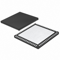
LTC2755CUP-12#TRPBF Linear Technology, LTC2755CUP-12#TRPBF Datasheet - Page 16

LTC2755CUP-12#TRPBF
Manufacturer Part Number
LTC2755CUP-12#TRPBF
Description
IC DAC 12BIT CUR OUT 64-QFN
Manufacturer
Linear Technology
Datasheet
1.LTC2755IUP-12PBF.pdf
(24 pages)
Specifications of LTC2755CUP-12#TRPBF
Settling Time
2µs
Number Of Bits
12
Data Interface
Parallel
Number Of Converters
4
Voltage Supply Source
Single Supply
Operating Temperature
0°C ~ 70°C
Mounting Type
Surface Mount
Package / Case
64-QFN
Lead Free Status / RoHS Status
Lead free / RoHS Compliant
Power Dissipation (max)
-
Available stocks
Company
Part Number
Manufacturer
Quantity
Price
LTC2755
OPERATION
System Offset Adjustment
Many systems require compensation for overall system
offset. The R
this purpose. For noise immunity and ease of adjustment,
the control voltage is attenuated to the DAC output:
V
V
spans]
V
The nominal input range of this pin is ±5V; other reference
voltages of up to ±15V may be used if needed. The R
pins have an input impedance of 1MΩ. To preserve the
settling performance of the LTC2755, drive this pin with a
Thevenin-equivalent impedance of 10k or less. Short any
unused R
16
OS
OS
OS
= –0.01 • V(R
= –0.04 • V(R
= –0.02 • V(R
VOSX
VOSX
system offset adjustment pins to GND.
offset adjustment pins are provided for
VOSX
VOSX
VOSX
) [0V to 5V, ±2.5V spans]
) [±10V span]
) [0V to 10V, ±5V, –2.5V to 7.5V
VOSX
Table 2. Span Codes
Codes not shown are reserved and should not be used.
Table 3. Address Codes
Codes not shown are reserved and should not be used.
*If readback is taken using the ALL DACs address, the LTC2755 defaults
to DAC A.
S2
0
0
0
0
1
1
A2
0
0
0
0
1
S1
0
0
1
1
0
0
A1
0
0
1
1
1
S0
0
1
0
1
0
1
SPAN
Unipolar 0V to 5V
Unipolar 0V to 10V
Bipolar –5V to 5V
Bipolar –10V to 10V
Bipolar –2.5V to 2.5V
Bipolar –2.5V to 7.5V
A0
0
1
0
1
1
DAC CHANNEL
ALL DACs*
DAC A
DAC B
DAC C
DAC D
2755f


