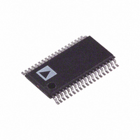
AD5346BRU Analog Devices Inc, AD5346BRU Datasheet

AD5346BRU
Specifications of AD5346BRU
Available stocks
Related parts for AD5346BRU
AD5346BRU Summary of contents
Page 1
FEATURES AD5346: octal 8-bit DAC AD5347: octal 10-bit DAC AD5348: octal 12-bit DAC Low power operation: 1.4 mA (max) @ 3.6 V Power-down to 120 400 Guaranteed monotonic by design over all ...
Page 2
AD5346/AD5347/AD5348 TABLE OF CONTENTS Specifications..................................................................................... 3 AC Characteristics............................................................................ 4 Timing Characteristics..................................................................... 5 Absolute Maximum Ratings............................................................ 6 ESD Caution.................................................................................. 6 AD5346 Pin Configurations and Function Descriptions ........... 7 AD5347 Pin Configurations and Function Descriptions ........... 8 AD5348 Pin Configurations and Function ...
Page 3
SPECIFICATIONS Table 2 5 REF unless otherwise noted 2 Parameter Min 3,4 DC PERFORMANCE AD5346 Resolution Relative Accuracy Differential Nonlinearity AD5347 Resolution Relative Accuracy Differential Nonlinearity AD5348 Resolution ...
Page 4
AD5346/AD5347/AD5348 2 Parameter Min 6 LOGIC OUTPUTS Output Low Voltage Output High Voltage – 2 3 Output Low Voltage, ...
Page 5
TIMING CHARACTERISTICS Table 2 5.5 V; all specifications T DD Parameter Limit at T Data Write Mode (Figure 4 ...
Page 6
AD5346/AD5347/AD5348 ABSOLUTE MAXIMUM RATINGS Table 25°C, unless otherwise noted A Parameter V to GND DD Digital Input Voltage to GND Digital Output Voltage to GND Reference Input Voltage to GND V to GND OUT Operating Temperature Range ...
Page 7
AD5346 PIN CONFIGURATIONS AND FUNCTION DESCRIPTIONS REF REF REF REF OUT 8-BIT AD5346 ...
Page 8
AD5346/AD5347/AD5348 AD5347 PIN CONFIGURATIONS AND FUNCTION DESCRIPTIONS REF REF V CD REF REF 10-BIT OUT AD5347 V B ...
Page 9
AD5348 PIN CONFIGURATIONS AND FUNCTION DESCRIPTIONS REF REF V CD REF REF 12-BIT OUT AD5348 ...
Page 10
AD5346/AD5347/AD5348 TERMINOLOGY Relative Accuracy For the DAC, relative accuracy or integral nonlinearity (INL measure of the maximum deviation, in LSBs, from a straight line passing through the actual endpoints of the DAC transfer function. Typical INL versus code ...
Page 11
Offset Error Drift This is a measure of the change in offset error with changes in temperature expressed in (ppm of full-scale range)/°C. Gain Error Drift This is a measure of the change in gain error with changes ...
Page 12
AD5346/AD5347/AD5348 TYPICAL PERFORMANCE CHARACTERISTICS 1 25° 0.5 0 –0.5 –1 100 150 CODE Figure 14. AD5346 Typical INL Plot 25° ...
Page 13
25°C 0.4 A MAX INL 0.3 0.2 MAX DNL 0.1 0 –0.1 MIN DNL –0.2 MIN INL –0.3 –0.4 –0 (V) REF Figure 20. AD5346 INL and DNL ...
Page 14
AD5346/AD5347/AD5348 1 REF GAIN = 1 UNBUFFERED 1 –40° 1.0 0 +105°C A 0.6 0.4 0.2 0 2.5 3.0 3.5 4.0 SUPPLY VOLTAGE Figure 26. Supply Current vs. Supply Voltage ...
Page 15
0.6 0.8 1.0 I (mA) DD Figure 32. I Histogram with and 2.50 2.49 2.48 2.47 1µs/DIV Figure ...
Page 16
AD5346/AD5347/AD5348 FUNCTIONAL DESCRIPTION The AD5346/AD5347/AD5348 are octal resistor-string DACs fabricated by a CMOS process with resolutions of 8, 10, and 12 bits, respectively. They are written to using a parallel interface. They operate from single supplies of 2 ...
Page 17
PARALLEL INTERFACE The AD5346/AD5347/AD5348 load their data as a single 8-, 10-, or 12-bit word. Double-Buffered Interface The AD5346/AD5347/AD5348 DACs all have double-buffered interfaces consisting of an input register and a DAC register. DAC data, BUF, and GAIN inputs are ...
Page 18
AD5346/AD5347/AD5348 The bias generator, the output amplifier, the resistor string, and all other associated linear circuitry are all shut down when the power-down mode is activated. However, the contents of the registers are unaffected when in power-down. The time to ...
Page 19
APPLICATIONS INFORMATION TYPICAL APPLICATION CIRCUITS The AD5346/AD5347/AD5348 can be used with a wide range of reference voltages, especially if the reference inputs are configured as unbuffered, in which case the devices offer full, one-quadrant multiplying capability over a reference range ...
Page 20
AD5346/AD5347/AD5348 DECODING MULTIPLE AD5346/AD5347/AD5348s The CS pin on these devices can be used in applications to decode a number of DACs. In this application, all DACs in the system receive the same data and WR pulses, but only the CS ...
Page 21
COARSE AND FINE ADJUSTMENT USING THE AD5346/AD5347/AD5348 Two of the DACs in the AD5346/AD5347/AD5348 can be paired together to form a coarse and fine adjustment function, as shown in Figure 47. As with the window comparator previously described, the description ...
Page 22
AD5346/AD5347/AD5348 Table 9. Overview of AD53xx Parallel Devices Part No. Resolution DNL SINGLES AD5330 8 ±0.25 AD5331 10 ±0.5 AD5340 12 ±1.0 AD5341 12 ±1.0 DUALS AD5332 8 ±0.25 AD5333 10 ±0.5 AD5342 12 ±1.0 AD5343 12 ±1.0 QUADS AD5334 ...
Page 23
OUTLINE DIMENSIONS 0.15 0.05 COPLANARITY PIN 1 INDICATOR 12° MAX 1.00 0.85 0.80 SEATING PLANE 9.80 9.70 9. 4.50 4.40 4. PIN 1 1.20 MAX 0.50 0.27 SEATING 0.20 BSC 0.17 PLANE 0.10 0.09 COMPLIANT TO ...
Page 24
... ORDERING GUIDES Table 11. AD5346 Ordering Guide Model Temperature Range AD5346BRU –40°C to +105°C AD5346BRU-REEL –40°C to +105°C AD5346BRU-REEL7 –40°C to +105°C AD5346BCP –40°C to +105°C AD5346BCP-REEL –40°C to +105°C AD5346BCP-REEL7 –40°C to +105°C Table 12. AD5347 Ordering Guide ...


