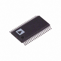
AD5346BRU Analog Devices Inc, AD5346BRU Datasheet - Page 10

AD5346BRU
Manufacturer Part Number
AD5346BRU
Description
IC DAC 8BIT OCTAL VOUT 38-TSSOP
Manufacturer
Analog Devices Inc
Datasheet
1.AD5348BRUZ.pdf
(24 pages)
Specifications of AD5346BRU
Rohs Status
RoHS non-compliant
Settling Time
6µs
Number Of Bits
8
Data Interface
Parallel
Number Of Converters
8
Voltage Supply Source
Single Supply
Power Dissipation (max)
8.3mW
Operating Temperature
-40°C ~ 105°C
Mounting Type
Surface Mount
Package / Case
38-TSSOP
Number Of Channels
8
Resolution
8b
Conversion Rate
167KSPS
Interface Type
Parallel
Single Supply Voltage (typ)
3.3/5V
Dual Supply Voltage (typ)
Not RequiredV
Architecture
Resistor-String
Power Supply Requirement
Single
Output Type
Voltage
Single Supply Voltage (min)
2.5V
Single Supply Voltage (max)
5.5V
Dual Supply Voltage (min)
Not RequiredV
Dual Supply Voltage (max)
Not RequiredV
Operating Temp Range
-40C to 105C
Operating Temperature Classification
Industrial
Mounting
Surface Mount
Pin Count
38
Lead Free Status / Rohs Status
Not Compliant
Available stocks
Company
Part Number
Manufacturer
Quantity
Price
Part Number:
AD5346BRUZ
Manufacturer:
ADI/亚德诺
Quantity:
20 000
AD5346/AD5347/AD5348
TERMINOLOGY
Relative Accuracy
For the DAC, relative accuracy or integral nonlinearity (INL) is
a measure of the maximum deviation, in LSBs, from a straight
line passing through the actual endpoints of the DAC transfer
function. Typical INL versus code plots can be seen in Figure 14,
Figure 15, and Figure 16.
Differential Nonlinearity
Differential nonlinearity (DNL) is the difference between the
measured change and the ideal 1 LSB change between any two
adjacent codes. A specified differential nonlinearity of ± 1 LSB
maximum ensures monotonicity. This DAC is guaranteed
monotonic by design. Typical DNL versus code plots can be
seen in Figure 17, Figure 18, and Figure 19.
Gain Error
This is a measure of the span error of the DAC, including any
error in the gain of the buffer amplifier. It is the deviation in
slope of the actual DAC transfer characteristic from the ideal
and is expressed as a percentage of the full-scale range. This is
illustrated in Figure 11.
Offset Error
This is a measure of the offset error of the DAC and the output
amplifier. It is expressed as a percentage of the full-scale range.
If the offset voltage is positive, the output voltage still positive at
zero input code. This is shown in Figure 12. Because the DACs
operate from a single supply, a negative offset cannot appear at
the output of the buffer amplifier. Instead, there is a code close
to zero at which the amplifier output saturates (amplifier
footroom). Below this code there is a dead band over which the
output voltage does not change. This is illustrated in Figure 13.
VOLTAGE
OUTPUT
DAC CODE
Figure 11. Gain Error
ACTUAL
IDEAL
POSITIVE
GAIN ERROR
NEGATIVE
GAIN ERROR
Rev. 0 | Page 10 of 24
POSITIVE
FOOTROOM
NEGATIVE
AMPLIFIER
OFFSET
VOLTAGE
OFFSET
NEGATIVE
OUTPUT
(~1mV)
OFFSET
VOLTAGE
OUTPUT
Figure 13. Negative Offset Error and Gain Error
Figure 12. Positive Offset Error and Gain Error
DEADBAND CODES
ACTUAL
DAC CODE
DAC CODE
IDEAL
IDEAL
ACTUAL
GAIN ERROR
AND
OFFSET
ERROR
GAIN ERROR
AND
OFFSET
ERROR


