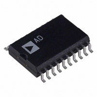
AD7948BR Analog Devices Inc, AD7948BR Datasheet - Page 10

AD7948BR
Manufacturer Part Number
AD7948BR
Description
IC DAC 12BIT MULTIPLYING 20-SOIC
Manufacturer
Analog Devices Inc
Datasheet
1.AD7943BNZ.pdf
(16 pages)
Specifications of AD7948BR
Rohs Status
RoHS non-compliant
Settling Time
600ns
Number Of Bits
12
Data Interface
Parallel
Number Of Converters
1
Voltage Supply Source
Single Supply
Power Dissipation (max)
25µW
Operating Temperature
-40°C ~ 85°C
Mounting Type
Surface Mount
Package / Case
20-SOIC (7.5mm Width)
Available stocks
Company
Part Number
Manufacturer
Quantity
Price
Part Number:
AD7948BR
Manufacturer:
ADI/亚德诺
Quantity:
20 000
Part Number:
AD7948BRSZ
Manufacturer:
ADI/亚德诺
Quantity:
20 000
Part Number:
AD7948BRSZ-REEL
Manufacturer:
ADI/亚德诺
Quantity:
20 000
Part Number:
AD7948BRZ
Manufacturer:
ADI/亚德诺
Quantity:
20 000
AD7943/AD7945/AD7948
Pin Mnemonic
I
AGND
DGND
CSMSB
DF/DOR
CTRL
DB7–DB0
LDAC
CSLSB
WR
V
V
R
OUT1
DD
REF
FB
Description
DAC current output terminal 1. Normally terminated at the virtual ground of output amplifier.
Analog Ground Pin. This pin connects to the back gates of the current steering switches. The DAC I
terminal is also connected internally to this point.
Digital Ground Pin.
Chip Select Most Significant Byte. Active Low Input. Used in combination with WR to load external data into
the input register or in combination with LDAC and WR to load external data into both input and DAC registers.
Data Format/Data Override. When this input is low, data in the DAC register is forced to one of two override
codes selected by CTRL. When the override signal is removed, the DAC output returns to reflect the value in
the DAC register. With DF/DOR high, CTRL selects either a left or right justified input data format. For normal
operation, DF/DOR is held high. See Table I.
Control Input. See DF/DOR description.
Digital Data Inputs.
Load DAC input, active low. This signal, in combination with others, is used to load the DAC register from
either the input register or the external data bus.
Chip Select Least Significant (LS) Byte. Active Low Input. Used in combination with WR to load external data
into the input register or in combination with WR and LDAC to load external data into both input and DAC
registers.
Write input, active low. This active low signal, in combination with others is used in loading external data into
the AD7948 input register and in transferring data from the input register to the DAC register.
Power supply input. This is nominally +5 V for Normal Mode Operation and +3.3 V to +5 V for Biased Mode
Operation.
DAC reference input.
DAC feedback resistor pin.
DF/DOR
0
0
1
1
WR
0
0
0
0
0
1
CSMSB
1
1
0
0
1
X
CTRL
0
1
0
1
Table I. Truth Table for DF/DOR CTRL
CSLSB
0
0
1
1
1
X
Table II. Truth Table for AD7948 Write Operation
AD7948 PIN FUNCTION DESCRIPTIONS
Function
DAC Register Contents Overridden by All 0s
DAC Register Contents Overridden by All 1s
Left-Justified Input Data Selected
Right-Justified Input Data Selected
LDAC
1
0
1
0
0
X
–10–
Function
Load LS Byte to Input Register
Load LS Byte to Input Register and DAC Register
Load MS Byte to Input Register
Load MS Byte to Input Register and DAC Register
Load Input Register to DAC Register
No Data Transfer
OUT2
REV. B


