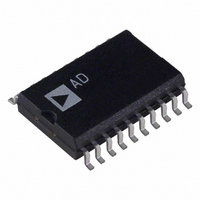
AD7948BR Analog Devices Inc, AD7948BR Datasheet - Page 4

AD7948BR
Manufacturer Part Number
AD7948BR
Description
IC DAC 12BIT MULTIPLYING 20-SOIC
Manufacturer
Analog Devices Inc
Datasheet
1.AD7943BNZ.pdf
(16 pages)
Specifications of AD7948BR
Rohs Status
RoHS non-compliant
Settling Time
600ns
Number Of Bits
12
Data Interface
Parallel
Number Of Converters
1
Voltage Supply Source
Single Supply
Power Dissipation (max)
25µW
Operating Temperature
-40°C ~ 85°C
Mounting Type
Surface Mount
Package / Case
20-SOIC (7.5mm Width)
Available stocks
Company
Part Number
Manufacturer
Quantity
Price
Part Number:
AD7948BR
Manufacturer:
ADI/亚德诺
Quantity:
20 000
Part Number:
AD7948BRSZ
Manufacturer:
ADI/亚德诺
Quantity:
20 000
Part Number:
AD7948BRSZ-REEL
Manufacturer:
ADI/亚德诺
Quantity:
20 000
Part Number:
AD7948BRZ
Manufacturer:
ADI/亚德诺
Quantity:
20 000
NORMAL MODE
1.23 V. V
characteristics are included for Design Guidance and are not subject to test.
AD7943/AD7945/AD7948
AC PERFORMANCE CHARACTERISTICS
0 V. V
cluded for Design Guidance and are not subject to test.
AC PERFORMANCE CHARACTERISTICS
BIASED MODE
Parameter
DYNAMIC PERFORMANCE
Specifications subject to change without notice.
Parameter
DYNAMIC PERFORMANCE
Specifications subject to change without notice.
Output Voltage Settling Time
Digital to Analog Glitch Impulse
Multiplying Feedthrough Error
Output Capacitance
Digital Feedthrough
Digital Feedthrough (AD7945, AD7948)
Total Harmonic Distortion
Output Noise Spectral Density
Output Voltage Settling Time
Digital to Analog Glitch Impulse
Multiplying Feedthrough Error
Output Capacitance
Digital Feedthrough (AD7943)
Digital Feedthrough (AD7945, AD7948) 5
Total Harmonic Distortion
Output Noise Spectral Density
@ 1 kHz
@ 1 kHz
REF
REF
= 6 V rms, 1 kHz sine wave; T
= 1 kHz, 2.45 V p-p, sine wave biased at 1.23 V; DAC output op amp is AD820; T
(AD7943: V
(AD7943: V
DD
DD
= +3 V to +5.5 V; V
= +4.5 V to +5.5 V; V
A
= T
MIN
to T
B Grades
600
60
–75
60
30
5
–83
35
MAX
IOUT1
5
60
–75
60
30
5
5
–83
25
A Grades
; DAC output op amp is AD843; unless otherwise noted.) These characteristics are in-
IOUT1
= V
= V
IOUT2
IOUT2
T Grade
700
60
–75
60
30
5
5
–83
35
= AGND = 1.23 V. AD7945, AD7948: V
= AGND = 0 V. AD7945, AD7948: V
nV-s typ
dB max
pF max
pF max
nV-s typ
nV-s typ
dB typ
nV/ Hz typ
Units
–4–
s typ
Units
ns typ
nV-s typ
dB max
pF max
pF max
nV-s typ
nV-s typ
dB typ
nV/ Hz typ All 1s Loaded to DAC. V
To 0.01% of Full-Scale Range. V
DAC Latch Alternately Loaded with All 0s and All 1s
V
with All 0s and All 1s
DAC Latch Loaded with All 0s
All 1s Loaded to DAC
All 0s Loaded to DAC
Feedthrough to the DAC Output with LD1, LD2
High and Alternate Loading of All 0s and All 1s
into the Input Shift Register
Feedthrough to the DAC Output with CS High
and Alternate Loading of All 0s and All 1s to the
DAC Bus
All 1s Loaded to DAC. V
Test Conditions/Comments
REF
= 1.23 V. DAC Register Alternately Loaded
A
= T
Test Conditions/Comments
To 0.01% of Full-Scale Range. V
+10 V; DAC Latch Alternately Loaded with
All 0s and All 1s
Measured with V
Alternately Loaded with All 0s and All 1s
DAC Latch Loaded with All 0s
All 1s Loaded to DAC
All 0s Loaded to DAC
Feedthrough to the DAC Output with LD1,
LD2 High and Alternate Loading of All 0s
and All 1s into the Input Shift Register
Feedthrough to the DAC Output with CS
High and Alternate Loading of All 0s and
All 1s to the DAC Bus
Op Amp Is OP07
MIN
to T
DD
DD
MAX
= +4.5 V to +5.5 V; V
= +3 V to +5.5 V; V
; unless otherwise noted.) These
REF
REF
= 0 V. DAC Latch
= 1.23 V
REF
REF
IOUT1
= 0 V
IOUT1
= 0 V. Output
= AGND =
=AGND =
REF
REV. B
=


