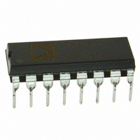
AD421BNZ Analog Devices Inc, AD421BNZ Datasheet - Page 6

AD421BNZ
Manufacturer Part Number
AD421BNZ
Description
IC DAC SNGL 16BIT 16-DIP
Manufacturer
Analog Devices Inc
Datasheet
1.AD421BRZRL.pdf
(14 pages)
Specifications of AD421BNZ
Data Interface
Serial
Settling Time
8µs
Number Of Bits
16
Number Of Converters
1
Voltage Supply Source
Single Supply
Power Dissipation (max)
1.95mW
Operating Temperature
-40°C ~ 85°C
Mounting Type
Through Hole
Package / Case
16-DIP (0.300", 7.62mm)
Resolution (bits)
16bit
Sampling Rate
125SPS
Input Channel Type
Serial
Supply Current
575µA
Digital Ic Case Style
DIP
No. Of Pins
16
Lead Free Status / RoHS Status
Lead free / RoHS Compliant
Available stocks
Company
Part Number
Manufacturer
Quantity
Price
Part Number:
AD421BNZ
Manufacturer:
ADI/亚德诺
Quantity:
20 000
CIRCUIT DESCRIPTION
The AD421 is designed for use in loop-powered 4–20 mA smart
transmitter applications. A smart transmitter, as a remote in-
strument, controls its current output signal on the same pair of
wires from which it receives its power. The AD421 essentially
provides three primary functions in the smart transmitter. These
functions are a DAC function for converting the microprocessor/
microcontroller’s digital data to analog format, a current amp-
lifier which sets the current flowing in the loop and a voltage
regulator to provide a stable operating voltage from the loop
supply. The part also contains a high speed serial interface, two
buffered output references and a clock oscillator circuit. The
different sections of the AD421 are discussed in more detail
below.
Voltage Regulator
The voltage regulator consists of an op amp, bandgap reference
and an external depletion mode FET pass transistor. This cir-
cuit is required to regulate the loop voltage that powers the
AD421 itself and the rest of the transmitter circuitry. Figure 3
shows the voltage regulator section of the AD421 plus the associ-
ated external circuitry for a V
The signal on the LV pin selects the voltage to which V
regulates by changing the gain of the resistor divider between
the op amp inverting input and the V
varies between COM and V
loop varies between 3 V and 5 V nominal. With LV connected
to COM, the regulated voltage is 5 V; with LV connected
through a 0.01 µF capacitor to V
3.3 V while if LV is connected to V
is 3 V.
The range of loop voltages that can be used by the configuration
shown in Figure 3 is determined by the FET breakdown and
saturation voltages. The external FET parameters such as Vgs
(off), I
amp output on the DRIVE pin can control the FET operating
point while swinging in the range from V
The main characteristics for selecting the FET pass transistor
are as follows:
AD421
Figure 3. AD421 Voltage Regulator Circuit to Provide
V
V
CC
CC
CIRCUITRY
TO EXTERNAL
AD421
= 3.3 V
DSS
REFERENCE
COM
BANDGAP
2.2 F
and transconductance must be chosen so that the op
LV
112.5k
0.01 F
1.21V
DN25D
121k
V
75k
134k
CC
CC
CC
, the voltage from the regulator
of 3.3 V.
CC
, the regulated voltage is
CC
CC
, the regulated voltage
DRIVE
COMP
CC
pin. As the LV pin
to COM.
0.01 F
1k
1000pF
LOOP(+)
CC
–6–
FET Type
I
BV
V
Power Dissipation
where V
the loop voltage.
The DN25D FET transistor from Supertex
requirements for the FET. Other suitable transistors include
ND2020L and ND2410L, both from Siliconix.
There are a number of external components required to com-
pensate the regulator loop and ensure stable operation. The
capacitor from the V
stabilize the regulator loop.
To provide additional compensation for the regulator loop, a
compensation capacitor of 0.01 µF should be connected
between the COMP and DRIVE pins and an external circuit
of a 1 kΩ resistor and a 1000 pF capacitor in series should be
connected between DRIVE and COM to stabilize this feed-
back loop formed with the regulator op amp and the external
pass transistor.
DAC Section
The AD421 contains a 16-bit sigma-delta DAC to convert the
digital information loaded to the input latch into a current. The
sigma-delta architecture is particularly useful for the relatively
low bandwidth requirements of the industrial control environ-
ment because of its inherent monotonicity at high resolution.
The AD421 guarantees monotonicity to the 16-bit level.
The sigma-delta DAC consists of a second order modulator
followed by a continuous time filter. The single bit stream from
the modulator controls a switched current source. This current
source is then filtered by three resistor-capacitor filter sections.
The resistors for each of the filter sections are on-chip while
the capacitors are external on the C1–C3 pins. To meet the
specified full-scale settling on the part, low dielectric absorption
capacitors (NPO) are required. Suitable values for these capacitors
are C1 = 0.01 µF, C2 = 0.01 µF, and C3 = 0.0033 µF.
Current Amplifier
The DAC output current drives the second section, an opera-
tional amplifier and NPN transistor which acts as a current
amplifier to set the current flowing through the LOOP RTN
pin. Figure 4 shows the current amplifier section of the AD421.
An 80 kΩ resistor connected between the DAC output and loop
return is used as a sampling resistor to determine current. The
base drive to the NPN transistor servos the voltage across the
40 Ω resistor to equal the voltage across the 80 kΩ resistor.
DSS
PINCHOFF
DS
CC
is the operating voltage of the AD421 and V
Table I. FET Characteristics
CC
pin to the COM pin is required to
N-Channel Depletion Mode
24 mA min
(V
V
24 mA × (V
CC
LOOP
max
– V
CC
LOOP
) min
1
– V
meets all the above
CC
) min
LOOP
REV. C
is


