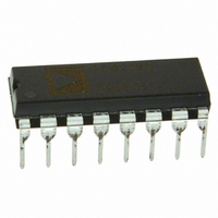
AD421BNZ Analog Devices Inc, AD421BNZ Datasheet - Page 8

AD421BNZ
Manufacturer Part Number
AD421BNZ
Description
IC DAC SNGL 16BIT 16-DIP
Manufacturer
Analog Devices Inc
Datasheet
1.AD421BRZRL.pdf
(14 pages)
Specifications of AD421BNZ
Data Interface
Serial
Settling Time
8µs
Number Of Bits
16
Number Of Converters
1
Voltage Supply Source
Single Supply
Power Dissipation (max)
1.95mW
Operating Temperature
-40°C ~ 85°C
Mounting Type
Through Hole
Package / Case
16-DIP (0.300", 7.62mm)
Resolution (bits)
16bit
Sampling Rate
125SPS
Input Channel Type
Serial
Supply Current
575µA
Digital Ic Case Style
DIP
No. Of Pins
16
Lead Free Status / RoHS Status
Lead free / RoHS Compliant
Available stocks
Company
Part Number
Manufacturer
Quantity
Price
Part Number:
AD421BNZ
Manufacturer:
ADI/亚德诺
Quantity:
20 000
of 11.147 mA. With 16 clock pulses between consecutive latch
signals data written is for normal 4 mA to 20 mA operation.
Alarm Current Coding
Table III shows the ideal input-code-to-output-current relation-
ship for alarm current programming of the AD421. In this case,
the equivalent span is 0 mA to 32 mA but a reliable operating
span is 3.5 mA to 24 mA. The part may give an indeterminate
output for code values outside the range given in the table. As a
result, the user is advised to restrict the code programmed to the
part in alarm current mode to within the range shown in Table
III. Figure 7 shows a timing diagram for loading an alarm cur-
rent of 3.75 mA to the AD421 with an 8-bit microcontroller
using three 8-bit writes.
The output current values shown assume a REF IN voltage of
+2.5 V. With a REF IN of +2.5 V, an ideal 1 LSB = 32 mA/
131,072 = 244 nA.
AD421
CLOCK
LATCH
DATA
Figure 6. Write Cycle for 4 mA to 20 mA Operation
Code
0000 0000 0000 0000
0000 0000 0000 0001
0000 0000 0000 0010
0100 0000 0000 0000
1000 0000 0000 0000
1100 0000 0000 0000
1111 1111 1111 1101
1111 1111 1111 1110
1111 1111 1111 1111
Code
0 0011 1000 0000 0000
0 0011 1100 0000 0000
0 0100 0000 0000 0000
0 1000 0000 0000 0000
1 0000 0000 0000 0000
1 0100 0000 0000 0000
1 0110 0000 0000 0000
1 1000 0000 0000 0000
1
Table II. Ideal Input/Output Code Table
for 4 mA to 20 mA Operation
Table III. Ideal Input/Output Code Table
for Alarm Current Operation
0 1 1
0
0
1
WORD "N"
0 0
1 1
1
Output Current
3.5 mA
3.75 mA
4 mA
8 mA
16 mA
20 mA
22 mA
24 mA
0 0
Output Current
4 mA
4.000244 mA
4.000488 mA
8 mA
12 mA
16 mA
19.999268 mA
19.999512 mA
19.999756 mA
1
1
WORD "N +1"
1
0 0 1
–8–
MICROPROCESSOR INTERFACING
AD421 – MC68HC11 (SPI BUS) INTERFACE
Figure 8 shows a typical interface between the AD421 and the
Motorola MC68HC11 SPI (Serial Peripheral Interface) bus.
The SCK, MOSI and SS pins of the 68HC11 are respectively
connected to the CLOCK, DATA IN and LATCH pins of the
AD421.
A typical routine such as the one shown below begins by initializ-
ing the state of the various SPI data and control registers.
INIT
NEXTPT LDAA MSBY
SENDAT LDY
WAIT1
WAIT2
The SPI data port is configured to process data in 8-bit bytes.
The most significant data byte (MSBY) is retrieved from
memory and processed by the SENDAT routine. The
driven low by indexing into the PORTD data register and clear
Bit 5. The MSBY is then sent to the SPI data register where it is
automatically transferred to the AD421 internal shift resistor.
CLOCK
LATCH
DATA
Figure 7. Write Cycle for Programming Alarm Current
Data
* ADDITIONAL PINS OMITTED FOR CLARITY
LDAA #$2F
STAA PORTD
LDAA #$38
STAA DDRD
LDAA #$50
STAA SPCR
BSR
JMP
BCLR $08,Y,$20 ;DRIVE SS (LATCH) LOW
STAA SPDR
LDAA SPSR
BPL
LDAA LSBY
STAA SPDR
LDAA SPSR
BPL
BSET
RTS
68HC11
X X X X X X X
Figure 8. AD421 to 68HC11 Interface
SENDAT ;JUMP TO DAC OUTPUT ROUTINE
NEXTPT ;INFINITE LOOP
#$1000
WAIT1
WAIT2;
$08,Y,$20 ;DRIVE SS HIGH TO LATCH DATA
MOSI
SCK
SS
0
0
;SS = 1; SCK = 0; MOSI = 1
;SEND TO SPI OUTPUTS
;SS, SCK, MOSI = OUTPUTS
;SEND DATA DIRECTION INFO
;DABL INTRPTS, SPI IS MASTER & ON
;CPOL = 0, CPHA = 0, 1MHZ BAUDRATE
;LOAD ACCUM W/UPPER 8 BITS
;POINT AT ON-CHIP REGISTERS
;SEND MS-BYTE TO SPI DATA REG
;CHECK STATUS OF SPIE
;POLL FOR END OF X-MISSION
;GET LOW 8 BITS FROM MEMORY
;SEND LS-BYTE TO SPI DATA REG
;CHECK STATUS OF SPIE
;POLL FOR END OF X-MISSION
WORD "N"
0
1
1
1 1
0
0
0
CLOCK
DATA IN
LATCH
0
0
0
0 0
AD421*
0
0
SS
REV. C
pin is


