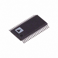
AD5547BRU Analog Devices Inc, AD5547BRU Datasheet - Page 18

AD5547BRU
Manufacturer Part Number
AD5547BRU
Description
IC DAC 16BIT DUAL 38-TSSOP
Manufacturer
Analog Devices Inc
Datasheet
1.AD5547BRUZ.pdf
(20 pages)
Specifications of AD5547BRU
Design Resources
Precision, Unipolar, Inverting Conversion Using AD5547/57 DAC (CN0026) Precision, Unipolar, Noninverting Configuration for the AD5547/57 DAC (CN0027) Precision, Bipolar, Configuration for AD5547/AD5557 DAC (CN0028)
Settling Time
500ns
Number Of Bits
16
Data Interface
Parallel
Number Of Converters
2
Voltage Supply Source
Single Supply
Power Dissipation (max)
55µW
Operating Temperature
-40°C ~ 125°C
Mounting Type
Surface Mount
Package / Case
38-TSSOP
Number Of Channels
2
Resolution
16b
Interface Type
Parallel
Single Supply Voltage (typ)
5V
Dual Supply Voltage (typ)
Not RequiredV
Architecture
R-2R
Power Supply Requirement
Single
Output Type
Current
Integral Nonlinearity Error
±2LSB
Single Supply Voltage (min)
2.7V
Single Supply Voltage (max)
5.5V
Dual Supply Voltage (min)
Not RequiredV
Dual Supply Voltage (max)
Not RequiredV
Operating Temp Range
-40C to 125C
Operating Temperature Classification
Automotive
Mounting
Surface Mount
Pin Count
38
Package Type
TSSOP
Lead Free Status / RoHS Status
Contains lead / RoHS non-compliant
Available stocks
Company
Part Number
Manufacturer
Quantity
Price
Part Number:
AD5547BRU
Manufacturer:
ADI/亚德诺
Quantity:
20 000
Part Number:
AD5547BRUZ
Manufacturer:
ADI/亚德诺
Quantity:
20 000
AD5547/AD5557
REFERENCE SELECTION
When selecting a reference for use with the AD55xx series of
current output DACs, pay attention to the output voltage,
temperature coefficient specification of the reference. Choosing
a precision reference with a low output temperature coefficient
minimizes error sources. Table 10 lists some of the references
available from Analog Devices, Inc., that are suitable for use
with this range of current output DACs.
AMPLIFIER SELECTION
The primary requirement for the current-steering mode is an
amplifier with low input bias currents and low input offset voltage.
Because of the code-dependent output resistance of the DAC,
the input offset voltage of an op amp is multiplied by the variable
gain of the circuit. A change in this noise gain between two
adjacent digital fractions produces a step change in the output
voltage due to the amplifier’s input offset voltage. This output
voltage change is superimposed upon the desired change in output
between the two codes and gives rise to a differential linearity error,
which, if large enough, can cause the DAC to be nonmonotonic.
Table 10. Suitable Analog Devices Precision References
Part No.
ADR01
ADR01
ADR02
ADR02
ADR03
ADR03
ADR06
ADR06
ADR420
ADR421
ADR423
ADR425
ADR431
ADR435
ADR391
ADR395
Table 11. Suitable Analog Devices Precision Op Amps
Part No.
OP97
OP1177
AD8675
AD8671
ADA4004-1
AD8603
AD8607
AD8605
AD8615
AD8616
Output Voltage (V)
10
10
5.0
5.0
2.5
2.5
3.0
3.0
2.048
2.50
3.00
5.00
2.500
5.000
2.5
5.0
Supply Voltage (V)
±2 to ±20
±2.5 to ±15
±5 to ±18
±5 to ±15
±5 to ±15
1.8 to 5
1.8 to 5
2.7 to 5
2.7 to 5
2.7 to 5
Initial Tolerance (%)
0.05
0.05
0.06
0.06
0.1
0.1
0.1
0.1
0.05
0.04
0.04
0.04
0.04
0.04
0.16
0.10
V
(μV)
25
60
75
75
125
50
50
65
65
65
OS
Maximum
I
(nA)
0.1
2
2
12
90
0.001
0.001
0.001
0.001
0.001
B
Maximum
Maximum Temperature
Drift (ppm/°C)
3
9
3
9
3
9
3
9
3
3
3
3
3
3
9
9
Rev. B | Page 18 of 20
0.1 Hz to 10 Hz
Noise (μV p-p)
0.5
0.4
0.1
0.077
0.1
2.3
2.3
2.3
2.4
2.4
The input bias current of an op amp also generates an offset at
the voltage output because of the bias current flowing in the
feedback resistor, R
Common-mode rejection of the op amp is important in voltage-
switching circuits because it produces a code-dependent error
at the voltage output of the circuit.
Provided that the DAC switches are driven from true wideband
low impedance sources (V
Consequently, the slew rate and settling time of a voltage-switching
DAC circuit is determined largely by the output op amp. To obtain
minimum settling time in this configuration, minimize capacitance
at the V
the DAC. This is done by using low input capacitance buffer
amplifiers and careful board design.
Analog Devices offers a wide range of amplifiers for both precision
dc and ac applications, as listed in Table 11 and Table 12.
REF
node (the voltage output node in this application) of
I
1
1
1
1
1
1
1
1
0.5
0.5
0.5
0.5
0.8
0.8
0.12
0.12
SS
(mA)
Supply Current (μA)
40
40
2000
2000
600
500
2300
3000
2000
1000
FB
.
Output Noise (μV p-p)
20
20
10
10
6
6
10
10
1.75
1.75
2
3.4
3.5
8
5
8
IN
and AGND), they settle quickly.
TSOT-5
MSOP-8, SOIC-8
TSOT-5
MSOP-8, SOIC-8
Package(s)
SOIC-8 , PDIP-8
MSOP-8, SOIC-8
MSOP-8, SOIC-8
MSOP-8, SOIC-8
SOIC-8, SOT-23-5
WLCSP-5, SOT-23-5
Package(s)
SOIC-8
TSOT-5, SC70-5
SOIC-8
TSOT-5, SC70-5
SOIC-8
TSOT-5, SC70-5
SOIC-8
TSOT-5, SC70-5
SOIC-8, MSOP-8
SOIC-8, MSOP-8
SOIC-8, MSOP-8
SOIC-8, MSOP-8
SOIC-8, MSOP-8
SOIC-8, MSOP-8
TSOT-5
TSOT-5


