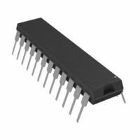
AD8582AN Analog Devices Inc, AD8582AN Datasheet - Page 3

AD8582AN
Manufacturer Part Number
AD8582AN
Description
IC DAC DUAL 12BIT 5V 24-DIP
Manufacturer
Analog Devices Inc
Datasheet
1.AD8582ARZ.pdf
(8 pages)
Specifications of AD8582AN
Rohs Status
RoHS non-compliant
Settling Time
16µs
Number Of Bits
12
Data Interface
Parallel
Number Of Converters
2
Voltage Supply Source
Single Supply
Power Dissipation (max)
35mW
Operating Temperature
-40°C ~ 85°C
Mounting Type
Through Hole
Package / Case
24-DIP (0.300", 7.62mm)
ABSOLUTE MAXIMUM RATINGS*
V
Logic Inputs to DGND . . . . . . . . . . . . . . . –0.3 V, V
V
V
AGND to DGND . . . . . . . . . . . . . . . . . . . . . . . . . –0.3 V, V
I
Package Power Dissipation . . . . . . . . . . . . . . . (T
Thermal Resistance,
Maximum Junction Temperature (T
Operating Temperature Range . . . . . . . . . . . . . –40 C to +85 C
Storage Temperature Range . . . . . . . . . . . . . –65 C to +150 C
Lead Temperature (Soldering, 10 sec) . . . . . . . . . . . . . +300 C
*Stresses above those listed under “Absolute Maximum Ratings” may cause
Model
AD8582AN
AD8582AR
AD8582Chips +25 C
*For die specifications contact your local Analog Devices sales office. The
CAUTION
ESD (electrostatic discharge) sensitive device. Electrostatic charges as high as 4000 V readily
accumulate on the human body and test equipment and can discharge without detection.
Although the AD8582 features proprietary ESD protection circuitry, permanent damage may
occur on devices subjected to high energy electrostatic discharges. Therefore, proper ESD
precautions are recommended to avoid performance degradation or loss of functionality.
REV. 0
permanent damage to the device. This is a stress rating only and functional
operation of the device at these or any other conditions above those indicated in the
operational sections of this specification is not implied. Exposure to absolute
maximum rating conditions for extended periods may affect device reliability.
OUT
AD8582 contains 1270 transistors.
DD
OUT
REF
24-Pin Plastic DIP Package (N-24) . . . . . . . . . . . . . 62 C/W
24-Lead SOIC Package (SOL-24) . . . . . . . . . . . . . . 73 C/W
to DGND & AGND . . . . . . . . . . . . . . . . . . . –0.3 V, +7 V
Short Circuit to GND . . . . . . . . . . . . . . . . . . . . . . 50 mA
to AGND . . . . . . . . . . . . . . . . . . . . . –0.3 V, V
to AGND . . . . . . . . . . . . . . . . . . . . . –0.3 V, V
LDA, LDB
D0–D11
V
RST
A/B
OUT
CS
ORDERING INFORMATION*
Temperature
–40 C to +85 C 24-Pin Plastic DIP N-24
–40 C to +85 C 24-Lead SOIC
Range
t
t
AS
DS
t
CSW
t
LS
JA
Timing Diagram
t
S
t
t
t
LH
DH
AH
Package
Description
Die
J
t
RSW
max) . . . . . . . . . . 150 C
t
S
t
LDW
± 1LSB
ERROR BAND
J
max–T
DD
DD
DD
Package
Option
SOL-24
+ 0.3 V
+ 0.3 V
+ 0.3 V
A
)/
DD
JA
–3–
Pin No. Name
1, 24
2
3
4, 21
5
6
7–18
19
20
22
23
V
DGND
AGND
OUTA
MSB
LDA
RST
DB0
DB1
DB2
DB3
DB4
DB5
24-Pin Plastic DIP
V
V
AGND
DGND Digital ground for input logic.
LDA,
LDB
MSB
RST
DB
CS
A/B
V
V
10
12
OUTA
OUTB
DD
REF
11
1
2
3
4
5
6
7
8
9
0–11
(Not to Scale)
TOP VIEW
AD8582
N-24
PIN CONFIGURATIONS
Description
Voltage outputs from the DACs. Fixed
output voltage range of 0 V to 4.095 V
with 1 mV/LSB. An internal
temperature stabilized reference
maintains a fixed full-scale voltage
independent of time, temperature and
power supply variations.
Analog Ground. Ground reference for
the internal bandgap reference voltage,
the DAC, and the output buffer.
Load DAC register strobes. Transfers
input register data to the DAC registers.
Active low inputs, Level sensitive latch.
May be connected together to double-
buffer load DAC registers.
Digital Input: High presets DAC
registers to half scale (800
clears DAC registers to zero (000
upon RST assertion.
Active low digital input that clears the
DAC register to zero, setting the DAC
to minimum scale when MSB pin = 0,
or half-scale when MSB pin = 1.
Twelve Binary Data Bit Inputs. DB11 is
the MSB and DB0 is the LSB.
Chip Select. Active low input.
Select DAC A = 0 or DAC B = 1.
Positive Supply. Nominal value +5 V, 5%.
Nominal 2.5 V reference output
voltage. This node must be buffered if
required to drive external loads.
PIN DESCRIPTION
17
24
23
22
21
20
19
18
16
15
14
13
DB11
DB10
DB9
DB8
DB7
DB6
V
V
V
LDB
A/B
CS
OUTB
REF
DD
WARNING!
24-Pin SOIC
12
(Not to Scale)
SOL-24
1
TOP VIEW
AD8582
ESD SENSITIVE DEVICE
H
), Low
AD8582
13
24
H
)


