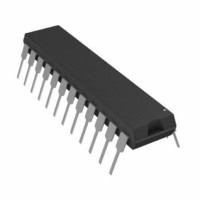
AD8582AN Analog Devices Inc, AD8582AN Datasheet - Page 4

AD8582AN
Manufacturer Part Number
AD8582AN
Description
IC DAC DUAL 12BIT 5V 24-DIP
Manufacturer
Analog Devices Inc
Datasheet
1.AD8582ARZ.pdf
(8 pages)
Specifications of AD8582AN
Rohs Status
RoHS non-compliant
Settling Time
16µs
Number Of Bits
12
Data Interface
Parallel
Number Of Converters
2
Voltage Supply Source
Single Supply
Power Dissipation (max)
35mW
Operating Temperature
-40°C ~ 85°C
Mounting Type
Through Hole
Package / Case
24-DIP (0.300", 7.62mm)
AD8582
CS
L
L
L
L
H
H
X
X
H
^Denotes positive edge triggered.
OPERATION
The AD8582 is a complete, ready-to-use dual 12-bit digital-to-
analog converter. Only one +5 V power supply is necessary for
operation. It contains two voltage-switched, 12-bit, laser-
trimmed digital-to-analog converters, a curvature-corrected
bandgap reference, rail-to-rail output op amps, input registers,
and DAC registers. The parallel data interface consists of twelve
data bits, DB0–DB11, an address select pin A/B, two load
strobe pins (LDA, LDB) and an active low CS strobe. In addi-
tion an asynchronous RST pin will set all DAC register bits to
zero causing the V
trimming applications when the MSB pin is programmed to
Logic 1. This function is useful for power on reset or system
failure recovery to a known state.
D/A CONVERTER SECTION
The internal DAC is a 12-bit voltage-mode device with an
output that swings from AGND potential to the 2.5 volt in-
ternal bandgap voltage. It uses a laser trimmed R-2R
ladder which is switched by N channel MOSFETs. The out-
put voltage of the DAC has a constant resistance independent
of digital input code. The DAC output (not available to the
user) is internally connected to the rail-to-rail output op amp.
AMPLIFIER SECTION
The internal DAC’s output is buffered by a low power con-
sumption precision amplifier. This low power amplifier contains
a differential PNP pair input stage which provides low offset
voltage and low noise, as well as the ability to amplify the zero-
scale DAC output voltages. The rail-to-rail amplifier is config-
ured in a gain of 1.6384 (= 4.095 V/2.5 V) in order to set the
4.095 volt full-scale output (1 mV/LSB). See Figure 3 for an
equivalent circuit schematic of the analog section.
The op amp has a 16 s typical settling time to 0.01%. There
are slight differences in settling time for negative slewing signals
versus positive. See the oscilloscope photos in the Typical Per-
formances section of this data sheet.
A/B
L
H
L
H
X
X
X
X
X
OUT
LDA
H
H
L
H
L
^
X
X
X
to become zero volts, or to midscale for
LDB
H
H
H
L
L
^
X
X
X
RST
H
H
H
H
H
H
L
L
^
Table I. Control Logic Truth Table
MSB
X
X
X
X
X
X
L
H
X
–4–
OUTPUT SECTION
The rail-to-rail output stage of this amplifier has been designed
to provide precision performance while operating near either
power supply. Figure 4 shows an equivalent output schematic of
the rail-to-rail amplifier with its N channel pull-down FETs that
will pull an output load directly to GND. The output sourcing
current is provided by a P channel pull-up device that can sup-
ply GND terminated loads, especially important at the –5%
supply tolerance value of 4.75 volts.
REFERENCE
BANDGAP
Input Register
Write to A
Write to B
Write to A
Write to B
Latched
Latched
Reset to Zero Scale
Reset to Midscale
Latch Reset Value
Figure 3. Equivalent Schematic of Analog Portion
Figure 4. Equivalent Analog Output Circuit
V
2.5V
REF
BUFFER
SWITCHES
N CH FET
VOLTAGE SWITCHED 12-BIT
SPDT
R-2R D/A CONVERTER
N-CH
P-CH
DAC Register
Latched
Latched
A Transparent
B Transparent
A & B Transparent
Latched
Reset to Zero Scale
Reset to Midscale
Latch Reset Value
2R
2R
2R
2R
R
R
2R
R1
V
V
AGND
OUT
DD
AV = 4.095/2.5
RAIL-TO-RAIL
OUTPUT
AMPLIFIER
R2
= 1.638V/V
REV. 0
V
OUT


