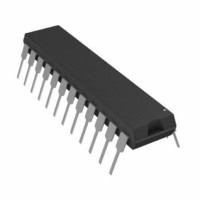
AD767KNZ Analog Devices Inc, AD767KNZ Datasheet - Page 2

AD767KNZ
Manufacturer Part Number
AD767KNZ
Description
IC DAC 12BIT 24-DIP
Manufacturer
Analog Devices Inc
Datasheet
1.AD767JNZ.pdf
(8 pages)
Specifications of AD767KNZ
Data Interface
Parallel
Settling Time
3µs
Number Of Bits
12
Number Of Converters
1
Voltage Supply Source
Dual ±
Operating Temperature
0°C ~ 70°C
Mounting Type
Through Hole
Package / Case
24-DIP (0.300", 7.62mm)
Resolution (bits)
12bit
Sampling Rate
500kSPS
Input Channel Type
Parallel
Supply Current
18mA
Digital Ic Case Style
DIP
No. Of Pins
24
Lead Free Status / RoHS Status
Lead free / RoHS Compliant
Power Dissipation (max)
-
Lead Free Status / RoHS Status
Lead free / RoHS Compliant, Lead free / RoHS Compliant
Available stocks
Company
Part Number
Manufacturer
Quantity
Price
Model
DIGITAL INPUTS
TRANSFER CHARACTERISTICS
DRIFT
CONVERSION SPEED
ANALOG OUTPUT
REFERENCE OUTPUT
POWER SUPPLY SENSITIVITY
POWER SUPPLY REQUIREMENTS
TEMPERATURE RANGE
NOTES
1
2
3
4
5
6
Specifications subject to change without notice.
Specifications shown in boldface are tested on all production units at final electrical test (except per Notes 1 and 2). Results from those tests are used to calculate
outgoing quality levels. All min and max specifications are guaranteed, although only those shown in boldface are tested on all production units.
AD767–SPECIFICATIONS
AD767 “S” specifications shown for information only. Consult Analog Devices Military Databook or contact factory for a controlled specification sheet.
AD767A Chips specifications are tested at +25 C and, when in boldface, at +85 C. They are typical at –25 C.
The digital input specifications are 100% tested at +25 C, and guaranteed but not tested over the full temperature range.
Adjustable to zero.
FSR means “Full-Scale Range” and is 20 V for 10 V range and 10 V for the 5 V range.
A minimum power supply of 12.5 V is required for a 10 V full-scale output and 11.4 V is required for all other voltage ranges.
Resolution
Logic Levels (TTL Compatible, T
ACCURACY
Gain T
Unipolar Offset T
Bipolar Zero T
Settling Time to 0.01% of FSR for
Ranges
Output Current
Short-Circuit Current
External Current
V
V
Rated Voltages
Range
Supply Current
Total Power Consumption
J/K
A/B
S
Operating
Storage (All Grades)
Output Impedance (dc)
CC
EE
V
V
V
I
I
Linearity Error @ +25 C
Differential Linearity Error @ +25 C
Gain Error
Unipolar Offset Error
Bipolar Zero Error
FSR change (2 k
For LSB Change
+11.4 to +16.5 V dc
–11.4 to –16.5 V dc
IH
IL
= –11.4 to –16.5 V dc
IH
IL
IL
= +11.4 to +16.5 V dc
T
T
with 10 k Feedback
with 5 k Feedback
Slew Rate
(V
(V
6
(Logic “0”) J, K, A, B
(Logic “0”) S
(Logic “1”)
A
A
A
6
IL
IH
= T
= T
= 25 C to T
= 0.8 V)
= 5.5 V)
MIN
MIN
4
A
to T
to T
= 25 C to T
A
= 25 C to T
MAX
MAX
4
MIN
500 pF load)
4
or T
MIN
MAX
MIN
or T
MIN
or T
MAX
–T
MAX
MAX
)
3
Min
+2.0
0
0
Monotonicity Guaranteed Monotonicity Guaranteed Monotonicity Guaranteed LSB
10
9.90
0.1
0
–25
–55
–55
–65
5
11.4
AD767J/A/S
(T
Typ
3
1
3
2
1
10.00
1.0
5
5
9
18
+5, +10
0.05
400
A
= +25 C,
1/2
1/2
1/2
0.1
1
0.05
5
1
5
2.5, 5, 10,
12, 15
1
Max
12
+5.5
+0.8
+0.7
10
5
4
3
40
10.10
10
10
13
23
600
+70
+85
+125
+125
+125
30
3
10
1
1
1
0.2
2
0.1
16.5
–2–
15 volt power supplies, Unipolar Mode, unless otherwise noted.)
Min
+2.0
0
10
9.90
0.1
0
–25
–55
–55
–65
5
11.4
AD767K/B
Typ
3
1
3
2
1
+5, +10
0.05
10.00
1.0
5
5
9
18
400
1/8
1/4
1/4
0.1
1
0.05
5
1
2.5, 5, 10,
12, 15
Max
12
+5.5
+0.8
10
5
4
3
40
10.10
10
10
13
23
+70
+85
+125
+125
600
+125
15
3
10
1/2
1/2
1
0.2
2
0.1
16.5
Min
+2.0
0
10
9.90
0.1
–25
–65
5
11.4
AD767A
Typ
3
1
3
2
1
+5, +10
10.00
1.0
5
5
9
18
400
0.05
1/2
1/2
1/2
0.1
1
0.05
5
1
5
2.5, 5, 10,
12, 15
2
Chips
Max
12
+5.5
+0.8
10
5
4
3
40
10.10
10
10
13
23
600
+85
+125
30
3
10
1
1
1
0.2
2
0.1
16.5
Bits
V
V
V
LSB
LSB
LSB
% of FSR
LSB
% of FSR
ppm of FSR/ C
ppm of FSR/ C
ppm of FSR/ C
V/ s
V
mA
mA
V
mA
ppm of FS/%
ppm of FS/%
V
V
mA
mA
mW
Units
C
C
C
C
C
A
A
s
s
s
REV. A
5


