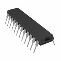
AD767KNZ Analog Devices Inc, AD767KNZ Datasheet - Page 3

AD767KNZ
Manufacturer Part Number
AD767KNZ
Description
IC DAC 12BIT 24-DIP
Manufacturer
Analog Devices Inc
Datasheet
1.AD767JNZ.pdf
(8 pages)
Specifications of AD767KNZ
Data Interface
Parallel
Settling Time
3µs
Number Of Bits
12
Number Of Converters
1
Voltage Supply Source
Dual ±
Operating Temperature
0°C ~ 70°C
Mounting Type
Through Hole
Package / Case
24-DIP (0.300", 7.62mm)
Resolution (bits)
12bit
Sampling Rate
500kSPS
Input Channel Type
Parallel
Supply Current
18mA
Digital Ic Case Style
DIP
No. Of Pins
24
Lead Free Status / RoHS Status
Lead free / RoHS Compliant
Power Dissipation (max)
-
Lead Free Status / RoHS Status
Lead free / RoHS Compliant, Lead free / RoHS Compliant
Available stocks
Company
Part Number
Manufacturer
Quantity
Price
REV. A
TIMING SPECIFICATIONS
(All Models, T
V
ABSOLUTE MAXIMUM RATINGS*
V
V
Digital Inputs (Pins 11, 13–24)
Ref In to Reference Ground . . . . . . . . . . . . . . . . . . . . . . 12 V
Bipolar Offset to Reference Ground . . . . . . . . . . . . . . . . 12 V
10 V Span R to Reference Ground . . . . . . . . . . . . . . . . . 12 V
20 V Span R to Reference Ground . . . . . . . . . . . . . . . . . 24 V
EE
CC
EE
to Power Ground . . . . . . . . . . . . . . . . . . . . –1.0 V to +7.0 V
= –12 V or –15 V)
to Power Ground . . . . . . . . . . . . . . . . . . . . . 0 V to –18 V
to Power Ground . . . . . . . . . . . . . . . . . . . . .0 V to +18 V
A
= 25 C, V
CC
= +12 V or +15 V,
DIP
Model
AD767JN
AD767JP
AD767KN Plastic DIP
AD767KP PLCC
AD767AD Ceramic DIP
AD767BD Ceramic DIP
AD767SD/
AD767A
NOTES
1
2
D = Ceramic DIP; N = Plastic DIP; P = Plastic Leaded Chip Carrier.
For details on grade and package offerings screened in accordance with MIL-STD-883, refer to
the Analog Devices Military Products Databook or current AD767/883B data sheet.
883B
Chips
1
Package
Plastic DIP
PLCC
Ceramic DIP
N/A
PIN CONFIGURATION
ORDERING GUIDE
Temperature Error Max
Range C
0 to +70
0 to +70
0 to +70
0 to +70
–25 to +85
–25 to +85
–55 to +125
–25 to +85
–3–
Ref Out, V
Power Dissipation . . . . . . . . . . . . . . . . . . . . . . . . . . . 1000 mW
*Stresses above those listed under “Absolute Maximum Ratings” may cause
Symbol Parameter
t
t
t
t
*t
DS
DH
CS
SETT
t
permanent damage to the device. This is a stress rating only and functional
operation of the device at these or any other conditions above those indicated in
the operational sections of this specification is not implied. Exposure to absolute
maximum rating conditions for extended periods may affect device reliability.
SETT
SETT
is measured referenced to the beginning of Data Valid.
is measured referenced to the leading edge of t
Linearity
T
Note 2
1 LSB
1 LSB
1/2 LSB
1/2 LSB
1 LSB
1/2 LSB
1 LSB
MIN
–T
Data Valid to End of CS
Data Hold Tiıne
CS Pulse Width
Output Voltage Settling Time* –
OUT
(–25 C to +85 C)
(–55 C to +125 C)
(–25 C to +85 C)
(–55 C to +125 C)
(–25 C to +85 C)
(–55 C to +125 C)
MAX
(Pins 6, 9) . . . Indefinite short to power ground
Gain T.C.
Max
ppm/ C
30
30
15
15
30
15
Note 2
30
PLCC
Momentary Short to V
CS
Min Typ Max
40
60
90
10
10
20
40
60
90
. If t
CS
AD767
–
–
–
–
–
–
–
–
–
2
> t
DS
, then
–
–
–
–
–
–
–
–
–
4
ns
ns
ns
ns
ns
ns
ns
ns
ns
CC
s


