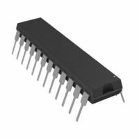
AD7225LNZ Analog Devices Inc, AD7225LNZ Datasheet

AD7225LNZ
Specifications of AD7225LNZ
Available stocks
Related parts for AD7225LNZ
AD7225LNZ Summary of contents
Page 1
FEATURES Four 8-bit DACs with output amplifiers Separate reference input for each DAC Microprocessor compatible with double-buffered inputs Simultaneous update of all 4 outputs Operates with single or dual supplies Extended temperature range operation No user trims required Skinny 24-lead ...
Page 2
AD7225 TABLE OF CONTENTS Features .............................................................................................. 1 Functional Block Diagram .............................................................. 1 General Description ......................................................................... 1 Product Highlights ........................................................................... 1 Revision History ............................................................................... 2 Specifications ..................................................................................... 3 Single Supply ................................................................................. 4 Absolute Maximum Ratings ............................................................ 5 ESD Caution .................................................................................. 5 ...
Page 3
SPECIFICATIONS −5 V ± 10%; AGND = DGND = unless otherwise noted. MIN MAX Table 1. Parameter STATIC PERFORMANCE Resolution Total Unadjusted ...
Page 4
AD7225 SINGLE SUPPLY ± 5 AGND = DGND = unless otherwise noted. Table 2. Parameter K, B Versions STATIC PERFORMANCE Resolution 8 Total Unadjusted Error 2 ±2 Differential Nonlinearity ...
Page 5
ABSOLUTE MAXIMUM RATINGS Table 3. Parameter V to AGND DGND AGND to DGND Digital Input Voltage to DGND AGND REF AGND 1 OUT Power Dissipation ...
Page 6
AD7225 PIN CONFIGURATIONS AND FUNCTION DESCRIPTIONS OUT OUT OUT OUT REF REF AD7225 REF ...
Page 7
TYPICAL PERFORMANCE CHARACTERISTICS T = 25° −5 V, unless otherwise noted 1.0 0.5 0 –0.5 –1 128 160 INPUT CODE Figure 4. Channel-to-Channel Matching 1.0 0.5 0 ...
Page 8
AD7225 TERMINOLOGY Total Unadjusted Error Total unadjusted error is a comprehensive specification that includes full-scale error, relative accuracy, and zero code error. Maximum output voltage is V − 1 LSB (ideal), where 1 LSB REF (ideal /256. The ...
Page 9
CIRCUIT INFORMATION DIGITAL-TO-ANALOG SECTION The AD7225 contains four identical, 8-bit voltage mode digital- to-analog converters. Each DAC has a separate reference input. The output voltages from the converters have the same polarity as the reference voltages, allowing single-supply operation. A ...
Page 10
AD7225 INTERFACE LOGIC INFORMATION The AD7225 contains two registers per DAC, an input register and a DAC register. The A0 and A1 address lines select which input register accepts data from the input port. When the WR signal is low, ...
Page 11
GROUND MANAGEMENT AND LAYOUT Because the AD7225 contains four reference inputs that can be driven from ac sources (see the AC Reference Signal section), careful layout and grounding is important to minimize analog crosstalk between the four channels. The dynamic ...
Page 12
AD7225 SPECIFICATION RANGES For the AD7225 to operate to rated specifications, its input reference voltage must be at least 4 V below the V supply voltage. This voltage differential is the overhead voltage required by the output amplifiers. The AD7225 ...
Page 13
UNIPOLAR OUTPUT OPERATION This is the basic mode of operation for each channel of the AD7225, with the output voltage having the same positive polarity The AD7225 can be operated single supply REF (V = AGND) or ...
Page 14
AD7225 BIPOLAR OUTPUT OPERATION Each of the DACs of the AD7225 can be individually confi- gured to provide bipolar output operation. This is possible using one external amplifier and two resistors per channel. Figure 17 shows a circuit used to ...
Page 15
AGND BIAS The AD7225 AGND pin can be biased above system ground (AD7225 DGND) to provide an offset zero analog output voltage level. Figure 18 shows a circuit configuration to achieve this for DAC Channel A of the AD7225. The ...
Page 16
AD7225 AC REFERENCE SIGNAL In some applications, it may be desirable to have ac reference signals. The AD7225 has multiplying capability within the upper (V − and lower (2 V) limits of reference voltage DD when operated with ...
Page 17
APPLICATIONS INFORMATION INPUT AD7820 AM29520 ADC TLC SAMPLES 10V AD584 AM7224 REF DAC V REF GAIN SET PROGRAMMABLE TRANSVERSAL FILTER A discrete time filter can be described by either multiplication in the frequency domain or by convolution in the time ...
Page 18
AD7225 less, there exists a good correlation with the actual performance of the transversal filter (see Figure 23). DIGITAL WORD MULTIPLICATION Because each DAC of the AD7225 has a separate reference input, the output of one DAC can be used ...
Page 19
MICROPROCESSER INTERFACE A15 ADDRESS BUS A8 8085A/ ADDRESS 8088 DECODE WR LATCH EN ALE AD7 ADDRESS DATA BUS AD0 *LINEAR CIRCUITRY OMITTED FOR CLARITY. Figure 25. AD7225-to-8085A/8088 Interface, Double-Buffered Mode A15 ADDRESS BUS A0 6809/ ADDRESS 6502 DECODE R/W EN ...
Page 20
AD7225 V GENERATION SS Operating the AD7225 from dual supplies results in enhanced performance over single-supply operation on a number of parameters as previously outlined. Some applications may require this enhanced performance, but may only have a single power supply ...
Page 21
OUTLINE DIMENSIONS 24 1 0.210 (5.33) MAX 0.150 (3.81) 0.130 (3.30) 0.115 (2.92) 0.022 (0.56) 0.018 (0.46) 0.014 (0.36) CONTROLLING DIMENSIONS ARE IN INCHES; MILLIMETER DIMENSIONS (IN PARENTHESES) ARE ROUNDED-OFF INCH EQUIVALENTS FOR REFERENCE ONLY AND ARE NOT APPROPRIATE FOR ...
Page 22
AD7225 0.048 (1.22) 0.042 (1.07) 4 0.048 (1.22) 5 0.042 (1.07) IDENTIFIER TOP VIEW (PINS DOWN 0.456 (11.582) 0.450 (11.430) 0.495 (12.57) 0.485 (12.32) 0.30 (0.0118) 0.10 (0.0039) COPLANARITY 0.10 0.180 (4.57) 0.165 (4.19) 0.056 (1.42) 0.020 (0.51) ...
Page 23
... AD7225KR-REEL −40°C to +85°C AD7225KRZ −40°C to +85°C AD7225KRZ-REEL −40°C to +85°C AD7225LN −40°C to +85°C AD7225LNZ −40°C to +85°C AD7225LP −40°C to +85°C AD7225LP-REEL −40°C to +85°C AD7225LPZ −40°C to +85°C AD7225LPZ-REEL − ...
Page 24
AD7225 NOTES ©2010 Analog Devices, Inc. All rights reserved. Trademarks and registered trademarks are the property of their respective owners. D00986-0-3/10(C) Rev Page ...


