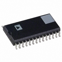
AD7244JR Analog Devices Inc, AD7244JR Datasheet - Page 4

AD7244JR
Manufacturer Part Number
AD7244JR
Description
IC DAC 14BIT LC2MOS DUAL 28SOIC
Manufacturer
Analog Devices Inc
Datasheet
1.AD7244JRZ.pdf
(12 pages)
Specifications of AD7244JR
Rohs Status
RoHS non-compliant
Settling Time
4µs
Number Of Bits
14
Data Interface
Serial
Number Of Converters
2
Voltage Supply Source
Dual ±
Power Dissipation (max)
205mW
Operating Temperature
-40°C ~ 85°C
Mounting Type
Surface Mount
Package / Case
28-SOIC (7.5mm Width)
Available stocks
Company
Part Number
Manufacturer
Quantity
Price
Part Number:
AD7244JR
Manufacturer:
ADI/亚德诺
Quantity:
20 000
Company:
Part Number:
AD7244JRZ
Manufacturer:
Analog Devices Inc
Quantity:
135
Part Number:
AD7244JRZ
Manufacturer:
ADI/亚德诺
Quantity:
20 000
AD7242/AD7244
TIMING CHARACTERISTICS
Parameter
t
t
t
t
t
t
NOTES
1
2
3
ABSOLUTE MAXIMUM RATINGS*
(T
V
V
AGND to DGND . . . . . . . . . . . . . . . . –0.3 V to V
V
REF OUT to AGND . . . . . . . . . . . . . . –0.3 V to V
REF INA, REF INB to AGND . . . . . . . –0.3 V to V
Digital Inputs to DGND . . . . . . . . . . . . –0.3 V to V
Operating Temperature Range
CAUTION
ESD (electrostatic discharge) sensitive device. Electrostatic charges as high as 4000 V readily
accumulate on the human body and test equipment and can discharge without detection.
Although the AD7242/AD7244 feature proprietary ESD protection circuitry, permanent damage
may occur on devices subjected to high energy electrostatic discharges. Therefore, proper ESD
precautions are recommended to avoid performance degradation or loss of functionality.
Timing specifications are sample tested at +25 C to ensure compliance. All input signals are specified with tr = tf = 5 ns (10% to 90% of 5 V) and timed from a volt-
See Figure 6.
TCLK Mark/Space ratio is 40/60 to 60/40.
1
2
3
4
5
6
age level of 1.6 V.
3
DD
SS
OUT
A
J, K Versions
A, B Versions . . . . . . . . . . . . . . . . . . . . . . . –40 C to +85 C
S Version . . . . . . . . . . . . . . . . . . . . . . . . . –55 C to +125 C
= +25 C unless otherwise noted)
to AGND . . . . . . . . . . . . . . . . . . . . . . . . . +0.3 V to –7 V
AD7244 . . . . . . . . . . . . . . . . . . . . . . . . . . . 0 C to +70 C
AD7242 . . . . . . . . . . . . . . . . . . . . . . . . . –40 C to +85 C
to AGND . . . . . . . . . . . . . . . . . . . . . . . . . –0.3 V to +7 V
to AGND . . . . . . . . . . . . . . . . . . . . . . . . . . . . V
Limit at T
(J, K, A, B Versions)
50
75
150
30
75
40
DIP
MIN
, T
MAX
1, 2
(V
DD
= +5 V
Limit at T
(S Version)
50
100
200
40
100
40
PIN CONFIGURATIONS
DD
DD
DD
DD
SS
+ 0.3 V
+ 0.3 V
+ 0.3 V
+ 0.3 V
to V
5%, V
MIN
DD
, T
SS
–4–
= –5 V
MAX
Storage Temperature Range . . . . . . . . . . . . –65 C to +150 C
Lead Temperature (Soldering, 10 sec) . . . . . . . . . . . . +300 C
Power Dissipation (Any Package) to +75 C . . . . . . . 550 mW
Derates above +75 C by . . . . . . . . . . . . . . . . . . . . . 6 mW/ C
*Stresses above those listed under “Absolute Maximum Ratings” may cause
permanent damage to the device. This is a stress rating only, functional operation
of the device at these or any other conditions above those listed in the operational
sections of this specification is not implied. Exposure to absolute maximum rating
conditions for extended periods may affect device reliability.
5%, AGND = DGND = 0 V)
Units
ns min
ns min
ns min
ns min
ns min
ns min
Conditions/Comments
TFS to TCLK Falling Edge
TCLK Falling Edge to TFS
TCLK Cycle Time
Data Valid to TCLK Setup Time
Data Valid to TCLK Hold Time
LDAC Pulse Width
SOIC
WARNING!
ESD SENSITIVE DEVICE
REV. A


