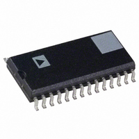
AD7244JR Analog Devices Inc, AD7244JR Datasheet - Page 6

AD7244JR
Manufacturer Part Number
AD7244JR
Description
IC DAC 14BIT LC2MOS DUAL 28SOIC
Manufacturer
Analog Devices Inc
Datasheet
1.AD7244JRZ.pdf
(12 pages)
Specifications of AD7244JR
Rohs Status
RoHS non-compliant
Settling Time
4µs
Number Of Bits
14
Data Interface
Serial
Number Of Converters
2
Voltage Supply Source
Dual ±
Power Dissipation (max)
205mW
Operating Temperature
-40°C ~ 85°C
Mounting Type
Surface Mount
Package / Case
28-SOIC (7.5mm Width)
Available stocks
Company
Part Number
Manufacturer
Quantity
Price
Part Number:
AD7244JR
Manufacturer:
ADI/亚德诺
Quantity:
20 000
Company:
Part Number:
AD7244JRZ
Manufacturer:
Analog Devices Inc
Quantity:
135
Part Number:
AD7244JRZ
Manufacturer:
ADI/亚德诺
Quantity:
20 000
AD7242/AD7244
CIRCUIT DESCRIPTION
The AD7242/AD7244 contains two 12-bit/14-bit D/A convert-
ers, each with an output buffer amplifier. The part also contains
a reference input buffer amplifier for each DAC, and an on-chip
3 V reference.
D/A Section
The AD7242/AD7244 contains two 12-bit/14-bit voltage mode
D/A converters, each consisting of highly stable thin-film resistors
and high speed single-pole, double-throw switches. The simplified
circuit diagram for the DAC section is shown in Figure 1. The
three MSBs of the data word are decoded to drive the seven
switches A-G. On the AD7242, the 9 LSBs switch a
Internal Reference
The on-chip reference is a temperature-compensated buried
Zener reference that is factory trimmed for 3 V
reference can be used to provide both the reference voltage for
the two D/A converters and the bipolar biasing circuitry. This is
achieved by connecting REF OUT to REF INA and REF INB.
The reference voltage can also be used for other components
and is capable of providing up to 500 A to an external load.
The maximum recommended capacitance on the reference
output pin for normal operation is 50 pF. If the reference
output is required to drive a capacitive load greater than 50 pF,
a 200
load. Decoupling the REF OUT pin with a series 200
and a parallel combination of a 10 F tantalum capacitor and a
0.1 F ceramic capacitor as in Figure 2 reduces the noise
spectral density of the reference (see Figure 4). Using this
decoupling scheme to generate the reference voltage for REF
INA and REF INB gives a channel-to-channel isolation number
of 110 dB (connecting REF OUT directly to REF INA and
REF INB gives 80 dB). The channel-to-channel isolation is 110
dB using an external reference.
External Reference
In some applications, the user may require a system reference or
some other external reference to drive the AD7242/AD7244
reference inputs. Figure 3 shows how the AD586 reference can
be conditioned to provide the 3 V reference required by the
AD7242/AD7244 reference inputs.
resistor should be placed in series with the capacitive
Figure 1. DAC Ladder Structure
10 mV. The
resistor
–6–
9-bit R-2R ladder structure while on the AD7244, the 11 LSBs
switch an 11-bit R-2R ladder structure. The output voltage
from this converter has the same polarity as the reference
voltage, REF IN.
The REF IN voltage is internally buffered by a unity gain
amplifier before being applied to the D/A converters and the
bipolar bias circuitry. The D/A converter is configured and
scaled for a 3 V reference, and the device is tested with 3 V
applied to REF IN. Operating the AD7242/AD7244 at refer-
ence voltages outside the 5% tolerance range may result in
degraded performance from the part.
Figure 2. Circuit Connection for REF OUT with an External
Capacitive Load of Greater Than 50 pF
Figure 3. AD586 Driving AD7242/AD7244 Reference Inputs
REV. A


