AD5764RCSUZ Analog Devices Inc, AD5764RCSUZ Datasheet - Page 12
AD5764RCSUZ
Manufacturer Part Number
AD5764RCSUZ
Description
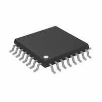
IC DAC QUAD 16BIT VOUT 32-TQFP
Manufacturer
Analog Devices Inc
Datasheet
1.AD5764RBSUZ.pdf
(32 pages)
Specifications of AD5764RCSUZ
Data Interface
Serial
Design Resources
High Accuracy, Bipolar Voltage Output Digital-to-Analog Conversion Using AD5764 (CN0006)
Settling Time
8µs
Number Of Bits
16
Number Of Converters
4
Voltage Supply Source
Dual ±
Power Dissipation (max)
275mW
Operating Temperature
-40°C ~ 85°C
Mounting Type
Surface Mount
Package / Case
32-TQFP, 32-VQFP
Resolution (bits)
16bit
Sampling Rate
1.26MSPS
Input Channel Type
Serial
Supply Voltage Range - Digital
2.7V To 5.25V
Supply Current
3.55mA
Digital Ic Case Style
QFP
Lead Free Status / RoHS Status
Lead free / RoHS Compliant
Available stocks
Company
Part Number
Manufacturer
Quantity
Price
Company:

Part Number:
AD5764RCSUZ
Manufacturer:
Analog Devices Inc
Quantity:
10 000
Company:
Part Number:
AD5764RCSUZ-REEL7
Manufacturer:
Analog Devices Inc
Quantity:
10 000


AD5764R
Pin No.
22
23
24
25
26
27
28
29
32
1
Internal pull-up device on this logic input. Therefore, it can be left floating; and it defaults to a logic high condition.
Mnemonic
VOUTB
VOUTA
AGNDA
REFAB
REFCD
REFOUT
REFGND
TEMP
BIN/2sCOMP
Analog Output Voltage of DAC B. Buffered output with a nominal full-scale output range of ±10 V. The output
amplifier is capable of directly driving a 10 kΩ, 200 pF load.
Analog Output Voltage of DAC A. Buffered output with a nominal full-scale output range of ±10 V. The output
amplifier is capable of directly driving a 10 kΩ, 200 pF load.
Ground Reference Pin for DAC A Output Amplifier.
External Reference Voltage Input for Channel A and Channel B. The reference input range is 1 V to 7 V, and it
programs the full-scale output voltage. V
External Reference Voltage Input for Channel C and Channel D. The reference input range is 1 V to 7 V, and it
programs the full-scale output voltage. V
Reference Output. This is the reference output from the internal voltage reference. The internal reference is 5 V ±
3 mV at 25°C, with a reference temperature coefficient of 10 ppm/°C.
Reference Ground Return for the Reference Generator and Buffers.
This pin provides an output voltage proportional to temperature. The output voltage is 1.47 V typical at 25°C die
temperature; variation with temperature is 5 mV/°C.
This pin determines the DAC coding. This pin should be hardwired to either DV
DV
(see Table 8).
Description
CC
, input coding is offset binary (see Table 7). When hardwired to DGND, input coding is twos complement
Rev. B | Page 12 of 32
REFIN
REFIN
= 5 V for specified performance.
= 5 V for specified performance.
CC
or DGND. When hardwired to
Related parts for AD5764RCSUZ
Image
Part Number
Description
Manufacturer
Datasheet
Request
R

Part Number:
Description:
±1.7g Dual-Axis IMEMS Accelerometer Evaluation Board
Manufacturer:
Analog Devices Inc
Datasheet:

Part Number:
Description:
Inertial Sensor Evaluation System
Manufacturer:
Analog Devices Inc
Datasheet:
Part Number:
Description:
Manufacturer:
Analog Devices Inc
Datasheet:
Part Number:
Description:
Manufacturer:
Analog Devices Inc
Datasheet:
Part Number:
Description:
Manufacturer:
Analog Devices Inc
Datasheet:
Part Number:
Description:
Manufacturer:
Analog Devices Inc
Datasheet:
Part Number:
Description:
Manufacturer:
Analog Devices Inc
Datasheet:
Part Number:
Description:
Manufacturer:
Analog Devices Inc
Datasheet:
Part Number:
Description:
Manufacturer:
Analog Devices Inc
Datasheet:
Part Number:
Description:
Manufacturer:
Analog Devices Inc
Datasheet:
Part Number:
Description:
Manufacturer:
Analog Devices Inc
Datasheet:
Part Number:
Description:
Manufacturer:
Analog Devices Inc
Datasheet:
Part Number:
Description:
Manufacturer:
Analog Devices Inc
Datasheet: