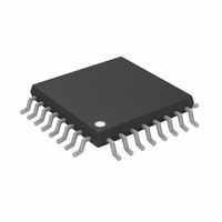
AD5764RCSUZ Analog Devices Inc, AD5764RCSUZ Datasheet - Page 26

AD5764RCSUZ
Manufacturer Part Number
AD5764RCSUZ
Description
IC DAC QUAD 16BIT VOUT 32-TQFP
Manufacturer
Analog Devices Inc
Datasheet
1.AD5764RBSUZ.pdf
(32 pages)
Specifications of AD5764RCSUZ
Data Interface
Serial
Design Resources
High Accuracy, Bipolar Voltage Output Digital-to-Analog Conversion Using AD5764 (CN0006)
Settling Time
8µs
Number Of Bits
16
Number Of Converters
4
Voltage Supply Source
Dual ±
Power Dissipation (max)
275mW
Operating Temperature
-40°C ~ 85°C
Mounting Type
Surface Mount
Package / Case
32-TQFP, 32-VQFP
Resolution (bits)
16bit
Sampling Rate
1.26MSPS
Input Channel Type
Serial
Supply Voltage Range - Digital
2.7V To 5.25V
Supply Current
3.55mA
Digital Ic Case Style
QFP
Lead Free Status / RoHS Status
Lead free / RoHS Compliant
Available stocks
Company
Part Number
Manufacturer
Quantity
Price
Company:
Part Number:
AD5764RCSUZ
Manufacturer:
Analog Devices Inc
Quantity:
10 000
Company:
Part Number:
AD5764RCSUZ-REEL7
Manufacturer:
Analog Devices Inc
Quantity:
10 000
AD5764R
OFFSET REGISTER
The offset register is addressed by setting the three REG bits to 101. The DAC address bits select the DAC channel with which the data
transfer takes place (see Table 10). The AD5764R offset register is an 8-bit register that allows the user to adjust the offset of each channel
by −16 LSBs to +15.875 LSBs in steps of one-eighth LSB, as shown in Table 18 and Table 19. The offset register coding is twos complement.
Table 18. Programming the Offset Register
REG2
1
Table 19. Offset Register Options
Offset Adjustment
+15.875 LSBs
+15.75 LSBs
No Adjustment (Default)
−15.875 LSBs
−16 LSBs
OFFSET AND GAIN ADJUSTMENT WORKED
EXAMPLE
Using the information provided in the Offset Register section,
the following worked examples demonstrate how the AD5764R
functions can be used to eliminate both offset and gain errors.
Because the AD5764R is factory calibrated, offset and gain errors
should be negligible. However, errors can be introduced by the
system within which the AD5764R is operating. For example,
a voltage reference value that is not equal to 5 V introduces
a gain error. An output range of ±10 V and twos complement
data coding are assumed.
Removing Offset Error
The AD5764R can eliminate an offset error in the range of
−4.88 mV to +4.84 mV with a step size of one-eighth of a
16-bit LSB.
1.
2.
3.
Number of Steps =
Offset Adjust Step Size =
The offset error measured is positive; therefore, a negative
adjustment of 16 steps is required. The offset register is
eight bits wide, and the coding is twos complement.
Calculate the step size of the offset adjustment, using the
following equation:
Measure the offset error by programming 0x0000 to the
data register and measuring the resulting output voltage.
For this example, the measured value is 614 μV.
Determine how many offset adjustment steps this value
represents, using the following equation:
REG1
0
Measured
REG0
1
Offset
Step
Offset
2
A2
16
20
DAC address
×
Size
8
Value
= 38.14 μV
A1
=
38
A0
614
OF7
0
0
0
1
1
.
14
μV
μV
DB15 to DB8
Don’t care
= 16 Steps
OF6
1
1
0
0
0
Rev. B | Page 26 of 32
OF5
1
1
0
0
0
DB7
OF7
The required offset register value can be calculated as follows:
1.
2.
3.
Note that this twos complement conversion is not necessary in
the case of a positive offset adjustment. The value to be pro-
grammed to the offset register is simply the binary representation
of the adjustment value.
Removing Gain Error
The AD5764R can eliminate a gain error at negative full-scale
output in the range of −9.77 mV to +9.46 mV with a step size of
one-half of a 16-bit LSB.
1.
2.
3.
The gain error measured is negative (in terms of magnitude).
Therefore, a positive adjustment of eight steps is required. The
gain register is six bits wide, and the coding is twos complement.
The required gain register value can be determined as follows:
1.
2.
Number of Steps =
Gain Adjust Step Size =
Convert the adjustment value to binary: 00010000.
Convert this binary value to a negative twos complement
number by inverting all bits and adding 1: 11110000.
Program this value, 11110000, to the offset register.
Calculate the step size of the gain adjustment, using the
following equation:
Measure the gain error by programming 0x8000 to the
data register and measuring the resulting output voltage.
The gain error is the difference between this value and −10 V.
For this example, the gain error is −1.2 mV.
Determine how many gain adjustment steps this value
represents, using the following equation:
Convert the adjustment value to binary: 001000.
Program this binary number to the gain register.
DB6
OF6
OF4
1
1
0
0
0
DB5
OF5
OF3
1
1
0
0
0
Measured
DB4
OF4
Gain
2
16
Step
20
OF2
1
1
0
0
0
Gain
×
DB3
OF3
2
Size
= 152.59 μV
Value
DB2
OF2
=
OF1
1
1
0
0
0
152
1
2 .
.
59
mV
DB1
OF1
μV
= 8 Steps
OF0
1
0
0
1
0
DB0
OF0


