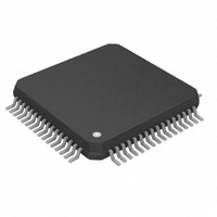
MAX5633UCB+D Maxim Integrated Products, MAX5633UCB+D Datasheet - Page 13

MAX5633UCB+D
Manufacturer Part Number
MAX5633UCB+D
Description
IC DAC 16BIT 32CH S&H 64-TQFP
Manufacturer
Maxim Integrated Products
Datasheet
1.MAX5633UCBD.pdf
(16 pages)
Specifications of MAX5633UCB+D
Number Of Bits
16
Data Interface
Serial
Number Of Converters
32
Voltage Supply Source
Dual ±
Operating Temperature
0°C ~ 85°C
Mounting Type
Surface Mount
Package / Case
64-LQFP
Lead Free Status / RoHS Status
Lead free / RoHS Compliant
Power Dissipation (max)
-
Settling Time
-
sequencer resumes normal operation at the interrupted
channel 7.
Burst Mode allows multiple SRAM locations to be
loaded at high speed. During Burst Mode, the output
voltages are not updated until the data burst is com-
plete and control returns to the sequencer. Select Burst
Mode by driving both IMMED and C1 low.
The sequencer is interrupted when CS is taken low. All
or part of the memory can be loaded while CS is low.
Each data word is loaded into its specified SRAM
address. The DAC conversion and SHA sample in
progress are completely transparent to the serial bus
activity. When CS is taken high, the sequencer resumes
scrolling at the interrupted SRAM address. New values
are updated when their turn comes up in the sequence.
After Burst Mode is used, it is recommended that at
least one full sequencer loop (320µs) is allowed to
occur before the serial port is accessed again. This
ensures that all outputs are updated before the
sequencer is interrupted.
Figure 6 shows an example of a burst mode operation.
As with the immediate update example, CS falls while
channel 7 is being refreshed. Data for multiple chan-
nels is loaded, and no channels are refreshed as long
as CS remains low. Once CS returns high, sequencing
resumes with channel 7 and continues normal refresh
operation. Thirty-three f
all channels have been updated.
An external clock may be used to control the
sequencer, altering the output update rate. The
sequencer runs at 1/4 the frequency of the supplied
clock (ECLK). The external clock option is selected by
driving either C0 or CLKSEL high.
When CLKSEL is asserted, the internal clock oscillator
is disabled. This feature allows synchronizing the
sequencer to other system operations, or shutting down
of the sequencer altogether during high-accuracy sys-
tem measurements. The low 1mV/s droop of these
devices ensures that no appreciable degradation of the
output voltages occurs, even during extended periods
of time when the sequencer is disabled.
A power-on reset (POR) circuit sets all channels to 0V
(code 4F2C hex) in sequence, requiring 320µs. This
prevents damage to downstream ICs due to arbitrary
reference levels being presented following system
power-up. This same function is available by driving
RST low. During the reset operation, the sequencer is
______________________________________________________________________________________
External Sequencer Clock
SEQ
cycles are required before
Power-On Reset
Burst Mode
16-Bit DACs with 32-Channel
Sample-and-Hold Outputs
run by the internal clock, regardless of the state of
CLKSEL. The reset process cannot be interrupted, seri-
al inputs will be ignored until the entire reset process is
complete.
Grounding and power-supply decoupling strongly influ-
ence device performance. Digital signals may couple
through the reference input, power supplies, and
ground connection. Proper grounding and layout can
reduce digital feedthrough and crosstalk. At the device
level, a 0.1µF capacitor is required for the V
and V
pins as possible. More substantial decoupling at the
board level is recommended and is dependent on the
number of devices on the board (Figure 7).
The MAX5631/MAX5632/MAX5633 have three separate
+5V logic power supplies, V
V
V
V
clock and SRAM. Additional filtering of V
V
TRANSISTOR COUNT: 16,229
PROCESS: BiCMOS
LDAC
LSHA
LOGIC
LSHA
L_
improves the overall performance of the device.
powers the control logic of the SHA array, and
powers the 16-bit digital-to-analog converter,
powers the serial interface, sequencer, internal
pins. They should be placed as close to the
Applications Information
Power Supplies and Bypassing
Chip Information
LDAC
, V
LOGIC
, and V
LDAC
DD
, V
LSHA
and
SS
13
,
.


