MAX5633UCB+D Maxim Integrated Products, MAX5633UCB+D Datasheet - Page 2
MAX5633UCB+D
Manufacturer Part Number
MAX5633UCB+D
Description
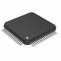
IC DAC 16BIT 32CH S&H 64-TQFP
Manufacturer
Maxim Integrated Products
Datasheet
1.MAX5633UCBD.pdf
(16 pages)
Specifications of MAX5633UCB+D
Number Of Bits
16
Data Interface
Serial
Number Of Converters
32
Voltage Supply Source
Dual ±
Operating Temperature
0°C ~ 85°C
Mounting Type
Surface Mount
Package / Case
64-LQFP
Lead Free Status / RoHS Status
Lead free / RoHS Compliant
Power Dissipation (max)
-
Settling Time
-


ABSOLUTE MAXIMUM RATINGS
V
V
V
V
REF to AGND............................................................-0.3V to +6V
GS to AGND................................................................V
CL and CH to AGND...................................................V
Logic Inputs to DGND ..............................................-0.3V to +6V
DGND to AGND........................................................-0.3V to +2V
Maximum Current Into OUT_ ............................................±10mA
16-Bit DACs with 32-Channel
Sample-and-Hold Outputs
ELECTRICAL CHARACTERISTICS
(V
CLKSEL = +5V, f
Stresses beyond those listed under “Absolute Maximum Ratings” may cause permanent damage to the device. These are stress ratings only, and functional
operation of the device at these or any other conditions beyond those indicated in the operational sections of the specifications is not implied. Exposure to
absolute maximum rating conditions for extended periods may affect device reliability.
2
DC CHARACTERISTICS
Resolution
Output Range
Offset Voltage
Offset Voltage Tempco
Gain Error
Gain Tempco
Integral Linearity Error
Differential Linearity Error
Maximum Output Drive Current
DC Output Impedance
Maximum Capacitive Load
DC Crosstalk
Power-Supply Rejection Ratio
DD
SS
DD
LDAC
DD
to AGND .........................................................-6.0V to +0.3V
_______________________________________________________________________________________
to AGND.......................................................-0.3V to +12.2V
to V
= +10V, V
, V
SS
LOGIC
PARAMETER
...........................................................................+15V
, V
SS
ECLK
LSHA
= -4V, V
= 400kHz, T
to AGND or DGND ..............-0.3V to +6V
LOGIC
A
= V
= T
SYMBOL
V
PSRR
R
DNL
I
LDAC
OUT_
INL
OUT
MIN
OUT
N
to T
= V
MAX
(Note 1)
Code = 4F2C hex
(Note 2)
V
V
guaranteed to 14 bits
Sinking and sourcing
MAX5631
MAX5632
MAX5633
MAX5631
MAX5632
MAX5633
Internal oscillator enabled (Note 3)
Internal oscillator enabled
LSHA
OUT_
OUT_
, unless otherwise noted. Typical values are at T
SS
SS
= +5V, V
= -3.25V to +7.6V
= -3.25V to +7.6V. Monotonicity
to V
to V
DD
DD
REF
CONDITIONS
= +2.5V, AGND = DGND = V
Maximum Current Into Logic Inputs .................................±20mA
Continuous Power Dissipation (T
Operating Temperature Range...............................0°C to +85°C
Maximum Junction Temperature .....................................+150°C
Storage Temperature Range .............................-65°C to +150°C
Lead Temperature (soldering, 10s) .................................+300°C
64-Pin TQFP (derate 13.3mW/°C above +70°C) ............1066mW
68-Pin QFN (derate 28.6mW/°C above +70°C) ..............2285mW
V
MIN
0.75
350
700
SS
16
±2
35
GS
A
+
= +25°C.)
A
= 0, R
= +70°C)
0.005
1000
TYP
±15
±50
500
250
-90
-80
±5
±1
50
10
10
L
≥ 10MΩ, C
0.015
MAX
V
±200
1300
650
2.4
±1
±4
65
DD
-
L
ppm/°C
= 50pF,
UNITS
%FSR
µV/°C
LSB
Bits
mA
mV
dB
dB
pF
nF
%
Ω
V
Related parts for MAX5633UCB+D
Image
Part Number
Description
Manufacturer
Datasheet
Request
R

Part Number:
Description:
MAX7528KCWPMaxim Integrated Products [CMOS Dual 8-Bit Buffered Multiplying DACs]
Manufacturer:
Maxim Integrated Products
Datasheet:
Part Number:
Description:
Single +5V, fully integrated, 1.25Gbps laser diode driver.
Manufacturer:
Maxim Integrated Products
Datasheet:
Part Number:
Description:
Single +5V, fully integrated, 155Mbps laser diode driver.
Manufacturer:
Maxim Integrated Products
Datasheet:
Part Number:
Description:
VRD11/VRD10, K8 Rev F 2/3/4-Phase PWM Controllers with Integrated Dual MOSFET Drivers
Manufacturer:
Maxim Integrated Products
Datasheet:
Part Number:
Description:
Highly Integrated Level 2 SMBus Battery Chargers
Manufacturer:
Maxim Integrated Products
Datasheet:
Part Number:
Description:
Current Monitor and Accumulator with Integrated Sense Resistor; ; Temperature Range: -40°C to +85°C
Manufacturer:
Maxim Integrated Products
Part Number:
Description:
TSSOP 14/A�/RS-485 Transceivers with Integrated 100O/120O Termination Resis
Manufacturer:
Maxim Integrated Products
Part Number:
Description:
TSSOP 14/A�/RS-485 Transceivers with Integrated 100O/120O Termination Resis
Manufacturer:
Maxim Integrated Products
Part Number:
Description:
QFN 16/A�/AC-DC and DC-DC Peak-Current-Mode Converters with Integrated Step
Manufacturer:
Maxim Integrated Products
Part Number:
Description:
TDFN/A/65V, 1A, 600KHZ, SYNCHRONOUS STEP-DOWN REGULATOR WITH INTEGRATED SWI
Manufacturer:
Maxim Integrated Products
Part Number:
Description:
Integrated Temperature Controller f
Manufacturer:
Maxim Integrated Products
Part Number:
Description:
SOT23-6/I�/45MHz to 650MHz, Integrated IF VCOs with Differential Output
Manufacturer:
Maxim Integrated Products
Part Number:
Description:
SOT23-6/I�/45MHz to 650MHz, Integrated IF VCOs with Differential Output
Manufacturer:
Maxim Integrated Products
Part Number:
Description:
EVALUATION KIT/2.4GHZ TO 2.5GHZ 802.11G/B RF TRANSCEIVER WITH INTEGRATED PA
Manufacturer:
Maxim Integrated Products
Part Number:
Description:
QFN/E/DUAL PCIE/SATA HIGH SPEED SWITCH WITH INTEGRATED BIAS RESISTOR
Manufacturer:
Maxim Integrated Products
Datasheet: