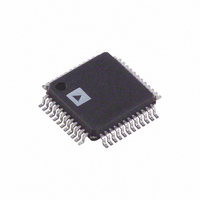
AD9772AAST Analog Devices Inc, AD9772AAST Datasheet - Page 19

AD9772AAST
Manufacturer Part Number
AD9772AAST
Description
IC DAC 14BIT 160MSPS 48-LQFP
Manufacturer
Analog Devices Inc
Series
TxDAC+®r
Datasheet
1.AD9772AASTZ.pdf
(40 pages)
Specifications of AD9772AAST
Rohs Status
RoHS non-compliant
Settling Time
11ns
Number Of Bits
14
Data Interface
Parallel
Number Of Converters
1
Voltage Supply Source
Analog and Digital
Power Dissipation (max)
272mW
Operating Temperature
-40°C ~ 85°C
Mounting Type
Surface Mount
Package / Case
48-LQFP
For Use With
AD9772A-EB - BOARD EVAL FOR AD9772A
Available stocks
Company
Part Number
Manufacturer
Quantity
Price
Company:
Part Number:
AD9772AAST
Manufacturer:
AD
Quantity:
996
Part Number:
AD9772AAST
Manufacturer:
ADI/亚德诺
Quantity:
20 000
Part Number:
AD9772AASTRL
Manufacturer:
ADI/亚德诺
Quantity:
20 000
Company:
Part Number:
AD9772AASTZ
Manufacturer:
TI
Quantity:
1 756
Company:
Part Number:
AD9772AASTZ
Manufacturer:
Analog Devices Inc
Quantity:
10 000
Part Number:
AD9772AASTZ
Manufacturer:
ADI/亚德诺
Quantity:
20 000
Company:
Part Number:
AD9772AASTZRL
Manufacturer:
Analog Devices Inc
Quantity:
10 000
Part Number:
AD9772AASTZRL
Manufacturer:
ADI/亚德诺
Quantity:
20 000
Zero-Stuffing Option Description
As shown in Figure 29, a zero or null in the frequency response
(after interpolation and DAC reconstruction) occurs at the final
DAC update rate (that is, 2× f
roll-off response of the DAC. In baseband applications, this roll-
off in the frequency response may not be as problematic
because much of the desired signal energy remains below
f
direct IF applications interested in extracting an image above
f
pass-band amplitude variation as well as the reduced signal
level of the higher images.
For instance, if the digital data into the AD9772A represents a
baseband signal centered around f
f
AD9772A experiences only a 0.18 dB amplitude variation over
its pass band, with the first image occurring at 7/4 × f
exhibiting 17 dB of attenuation relative to the fundamental.
However, if the high-pass filter response is selected, the AD9772A
produces pairs of images at [(2N + 1) × f
N = 0, 1, and so on. Note that due to the sin(x)/x response of the
DAC, only the lower or upper sideband images centered around
f
−6.54 dB and have a pass-band amplitude roll-off of 0.6 dB and
1.3 dB, respectively.
To improve on the pass-band flatness of the desired image
and/or to extract higher images (that is, 3 × f
the zero-stuffing option should be employed by bringing the
MOD1 pin high. This option increases the effective DAC
update rate by another factor of 2 because a midscale sample
(that is, 10 0000 0000 0000) is inserted after every data sample
originating from the 2× interpolation filter. A digital multiplexer
switching at a rate of 4 × f
output and a data register containing the midscale data sample is
used as shown in Figure 28 to implement this option. Therefore,
the DAC output is now forced to return to its differential midscale
current value (that is, I
each data sample from the digital filter.
DATA
DATA
DATA
DATA
Figure 29. Effects of Zero-Stuffing on the Sin(x)/x Response of the DAC
/2 and the amplitude variation is not as severe. However, in
/2, this roll-off may be problematic due to the increased
/10, the reconstructed baseband signal output from the
may be useful, although they are attenuated by −2.1 dB and
–10
–20
–30
–40
BASEBAND
0
REGION
0
0.5
ZERO-STUFFING
WITHOUT
1.0
OUTA
DATA
− I
FREQUENCY (
1.5
between the interpolation filter
OUTB
DATA
at 0 mA) after reconstructing
) due to the inherent sin(x)/x
2.0
DATA
WITH
ZERO-STUFFING
f
DATA
/4 with a pass band of
2.5
DATA
)
3.0
] ± f
DATA
DATA
± f
3.5
FUNDAMENTAL
/4, where
DATA
4.0
and
Rev. C | Page 19 of 40
),
The net effect is to increase the DAC update rate such that the
zero in the sin(x)/x frequency response occurs at 4 × f
accompanied by a corresponding reduction in output power as
shown in Figure 29. Note that if the high-pass response of the
2× interpolation filter is also selected, this action can be
modeled as a quarter-wave digital mixing process, because this
is equivalent to digitally mixing the impulse response of the
low-pass filter with a square wave having a frequency of exactly
f
It is important to realize that the zero-stuffing option by itself
does not change the location of the images, but rather changes
their signal level, amplitude flatness, and relative weighting. For
instance, in the previous example, the pass-band amplitude
flatness of the lower and upper sideband images centered
around f
while the signal level changes to −6.5 dBFS and −7.5 dBFS. The
lower or upper sideband image centered around 3 × f
exhibit an amplitude flatness of 0.77 dB and 1.29 dB with signal
levels of approximately −14.3 dBFS and −19.2 dBFS.
PLL CLOCK MULTIPLIER OPERATION
The phase-lock loop (PLL) clock multiplier circuitry, along with
the clock distribution circuitry, can produce the necessary
internally synchronized 1×, 2×, and 4× clocks for the edge-
triggered latches, 2× interpolation filter, zero-stuffing
multiplier, and DAC. Figure 30 shows a functional block
diagram of the PLL clock multiplier, which consists of a phase
detector, a charge pump, a voltage controlled oscillator (VCO),
a prescaler, and digital control input/output. The clock
distribution circuitry generates all the internal clocks for a given
mode of operation. The charge pump and VCO are powered
from PLLVDD, and the differential clock input buffer, phase
detector, prescaler, and clock distribution circuitry are powered
from CLKVDD. To ensure optimum phase noise performance
from the PLL clock multiplier and clock distribution circuitry,
PLLVDD and CLKVDD must originate from the same clean
analog supply.
DATA
CLKCOM
CLKVDD
OUT1×
(that is, f
Figure 30. Clock Multiplier with PLL Clock Multiplier Enabled
DATA
PLLLOCK
DISTRIBUTION
are improved to 0.14 dB and 0.24 dB, respectively,
CLOCK
DAC
/4).
CLK+
+
CLOCK CONTROL
CLK–
–
PRESCALER
DETECTOR
EXT/INT
PHASE
CHARGE
PUMP
AD9772A
VCO
AD9772A
PLLCOM
PLLVDD
DATA
DATA
LPF
DNC
2.7V
TO
3.6V


