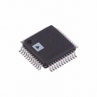
AD9772AAST Analog Devices Inc, AD9772AAST Datasheet - Page 32

AD9772AAST
Manufacturer Part Number
AD9772AAST
Description
IC DAC 14BIT 160MSPS 48-LQFP
Manufacturer
Analog Devices Inc
Series
TxDAC+®r
Datasheet
1.AD9772AASTZ.pdf
(40 pages)
Specifications of AD9772AAST
Rohs Status
RoHS non-compliant
Settling Time
11ns
Number Of Bits
14
Data Interface
Parallel
Number Of Converters
1
Voltage Supply Source
Analog and Digital
Power Dissipation (max)
272mW
Operating Temperature
-40°C ~ 85°C
Mounting Type
Surface Mount
Package / Case
48-LQFP
For Use With
AD9772A-EB - BOARD EVAL FOR AD9772A
Available stocks
Company
Part Number
Manufacturer
Quantity
Price
Company:
Part Number:
AD9772AAST
Manufacturer:
AD
Quantity:
996
Part Number:
AD9772AAST
Manufacturer:
ADI/亚德诺
Quantity:
20 000
Part Number:
AD9772AASTRL
Manufacturer:
ADI/亚德诺
Quantity:
20 000
Company:
Part Number:
AD9772AASTZ
Manufacturer:
TI
Quantity:
1 756
Company:
Part Number:
AD9772AASTZ
Manufacturer:
Analog Devices Inc
Quantity:
10 000
Part Number:
AD9772AASTZ
Manufacturer:
ADI/亚德诺
Quantity:
20 000
Company:
Part Number:
AD9772AASTZRL
Manufacturer:
Analog Devices Inc
Quantity:
10 000
Part Number:
AD9772AASTZRL
Manufacturer:
ADI/亚德诺
Quantity:
20 000
AD9772A
AD9772A EVALUATION BOARD
The AD9772A-EB is an evaluation board for the AD9772A
TxDAC. Careful attention to the layout and circuit design,
along with the prototyping area, allows the user to easily and
effectively evaluate the AD9772A in different modes of operation.
Referring to Figure 60 and Figure 61, the performance of
AD9772A can be evaluated differentially or in a single-ended
fashion using a transformer, differential amplifier, or directly
coupled output. To evaluate the output differentially using the
transformer, remove Jumper JP12 and Jumper JP13 and
monitor the output at J6 (IOUT). To evaluate the output
differentially, remove the transformer (T2) and install jumpers
JP12 and JP13. The output of the amplifier can be evaluated at
J13 (AMPOUT). To evaluate the AD9772A in a single-ended
fashion with a directly coupled output, remove the transformer
and Jumper JP12 and Jumper JP13, and install Resistor R16 or
Resistor R17 with 0 Ω.
The digital data to the AD9772A comes across a ribbon cable
that interfaces to a 40-pin IDC connector. Proper termination
or voltage scaling can be accomplished by installing the RN2
and/or RN3 SIP resistor networks. The 22 Ω DIP resistor
network, RN1, must be installed and helps reduce the digital
data edge rates. A single-ended clock input can be supplied via
the ribbon cable by installing JP8, or, more preferably, via the
SMA connector, J3 (CLOCK). If the clock is supplied by J3, the
AD9772A can be configured for a differential clock interface by
installing Jumper JP1 and configuring JP2, JP3, and JP9 in the
DF position. To configure the AD9772A clock input for a
single-ended clock interface, remove JP1 and configure JP2,
JP3, and JP9 in the SE position.
Rev. C | Page 32 of 40
The AD9772A PLL clock multiplier can be disabled by config-
uring Jumper JP5 in the L position. In this case, the user must
supply a clock input at twice (2×) the data rate via J3 (CLOCK).
The 1× clock is available on the SMA connector J1 (PLLLOCK),
and should be used to trigger a pattern generator directly or via
a programmable pulse generator. Note that PLLLOCK is capable
of providing a 0 V to 0.85 V output into a 50 Ω load. To enable
the PLL clock multiplier, JP5 must be configured for the
H position. In this case, the clock can be supplied via the ribbon
cable (that is, JP8 installed) or J3 (CLOCK). The divide-by-N
ratio can be set by configuring JP6 (DIV0) and JP7 (DIV1).
The AD9772A can be configured for baseband or direct IF
mode operation by configuring Jumper JP11 (MOD0) and
Jumper JP10 (MOD1). For baseband operation, JP10 and JP11
should be configured in the L position. For direct IF operation,
JP10 and JP11 should be configured in the H position. For direct
IF operation without zero-stuffing, JP11 should be configured in
the H position while JP10 should be configured in the low position.
The AD9772A voltage reference can be enabled or disabled via
JP4. To enable the reference, configure JP4 in the internal position.
A voltage of approximately 1.2 V will appear at the TP6 (REFIO)
test point. To disable the internal reference, configure JP4 in the
external position and drive TP6 with an external voltage reference.
Lastly, the AD9772A can be placed in the sleep mode by driving
the TP11 test point with a logic level high input signal.


