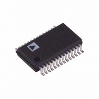
AD5554BRS Analog Devices Inc, AD5554BRS Datasheet - Page 15

AD5554BRS
Manufacturer Part Number
AD5554BRS
Description
IC DAC 14BIT QUAD SERIAL 28-SSOP
Manufacturer
Analog Devices Inc
Datasheet
1.AD5554BRSZ.pdf
(16 pages)
Specifications of AD5554BRS
Rohs Status
RoHS non-compliant
Settling Time
2µs
Number Of Bits
14
Data Interface
Serial
Number Of Converters
4
Voltage Supply Source
Dual ±
Power Dissipation (max)
1.25mW
Operating Temperature
-40°C ~ 85°C
Mounting Type
Surface Mount
Package / Case
28-SSOP
Available stocks
Company
Part Number
Manufacturer
Quantity
Price
Part Number:
AD5554BRSZ
Manufacturer:
ADI/亚德诺
Quantity:
20 000
Layout and Power Supply Bypassing
It is good practice to employ a compact, minimum lead length
layout design. The leads to the input should be as direct as possible
with a minimum conductor length. Ground paths should have
low resistance and low inductance.
Similarly, it is good practice to bypass the power supplies with
quality capacitors for optimum stability. Supply leads to the device
should be bypassed with 0.01 μF to 0.1 μF disc or chip ceramic
capacitors. Low ESR 1 μF to 10 μF tantalum or electrolytic capaci-
tors should also be applied at V
disturbance and filter any low frequency ripple (see Figure 24).
Users should not apply switching regulators for V
power supply rejection ratio (PSRR) degradation over frequency.
Grounding
The DGND and A
digital and analog ground references. To minimize the digital
ground bounce, the DGND terminal should be joined remotely
at a single point to the analog ground plane (see Figure 24).
APPLICATIONS
The AD5544/AD5554 are, inherently, two-quadrant multiplying
DACs. That is, they can be easily set up for unipolar output
operation. The full-scale output polarity is the inverse of the
reference input voltage.
Figure 24. Power Supply Bypassing and Grounding Connection
V
V
DD
SS
10µF
10µF
GND
C3
C4
x pins of the AD5544/AD5554 serve as
+
0.1µF
0.1µF
C1
C2
DD
to minimize any transient
AD5544/AD5554
V
A
V
DD
GND
SS
X
DGND
DD
due to the
Rev. D | Page 15 of 16
In some applications, it may be necessary to generate the full
four-quadrant multiplying capability or a bipolar output swing.
This is easily accomplished using an additional external ampli-
fier (A2) configured as a summing amplifier (see Figure 25).
In this circuit, the first and second amplifiers (A1 and A2)
provide a total gain of 2, which increases the output voltage span
to 20 V. Biasing the external amplifier with a 10 V offset from
the reference voltage results in a full four-quadrant multiplying
circuit. The transfer equation of this circuit shows that both
negative and positive output voltages are created as the input
data (D) is incremented from code zero (V
midscale (V
V
V
10V
AD588
OUT
OUT
V
DIGITAL INTERFACE CONNECTIONS
OMITTED FOR CLARITY.
REF
Figure 25. Four-Quadrant Multiplying Application Circuit
⎛
⎜
⎝
⎛
⎜
⎝
OUT
32768
8192
V
D
DD
D
= 0 V) to full scale (V
V
ONE CHANNEL
SS
−
AD5544
−
1
1
⎞
⎟
⎠
V
A
⎞
⎟
⎠
×
REF
GND
×
−
X
F
−
V
V
REF
R
REF
A
FB
GND
10kΩ
X
(
5kΩ
for
I
(
OUT
X
for
X
the
OUT
the
AD5544/AD5554
AD
= 10 V).
A2
A1
AD
–10V < V
10kΩ
OUT
5554
5544
= −10 V) to
OUT
)
)
< +10V
V
OUT
(3)
(4)


