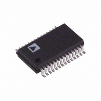
AD5554BRS Analog Devices Inc, AD5554BRS Datasheet - Page 5

AD5554BRS
Manufacturer Part Number
AD5554BRS
Description
IC DAC 14BIT QUAD SERIAL 28-SSOP
Manufacturer
Analog Devices Inc
Datasheet
1.AD5554BRSZ.pdf
(16 pages)
Specifications of AD5554BRS
Rohs Status
RoHS non-compliant
Settling Time
2µs
Number Of Bits
14
Data Interface
Serial
Number Of Converters
4
Voltage Supply Source
Dual ±
Power Dissipation (max)
1.25mW
Operating Temperature
-40°C ~ 85°C
Mounting Type
Surface Mount
Package / Case
28-SSOP
Available stocks
Company
Part Number
Manufacturer
Quantity
Price
Part Number:
AD5554BRSZ
Manufacturer:
ADI/亚德诺
Quantity:
20 000
Parameter
SUPPLY CHARACTERISTICS
AC CHARACTERISTICS
1
2
3
4
TIMING DIAGRAMS
All static performance tests (except I
tied to the amplifier output. Typical values represent average readings measured at 25°C.
These parameters are guaranteed by design and not subject to production testing.
All input control signals are specified with t
All ac characteristic tests are performed in a closed-loop system using an
Data Setup
Data Hold
Load Setup
Load Hold
Power Supply Range
Positive Supply Current
Negative Supply Current
Power Dissipation
Power Supply Sensitivity
Output Voltage Settling Time
Reference Multiplying BW
DAC Glitch Impulse
Feedthrough Error
Crosstalk Error
Digital Feedthrough
Total Harmonic Distortion
Output Spot Noise Voltage
4
LDAC
LDAC
CLK
CLK
SDI
SDI
CS
CS
OUT
) are performed in a closed-loop system using an external precision
A1
A1
Symbol
t
t
t
t
V
I
I
P
PSS
t
BW − 3 dB
Q
V
V
Q
THD
e
DD
SS
DS
DH
LDS
LDH
S
t
t
DISS
N
DD RANGE
OUT
OUT
CSS
CSS
R
= t
A0
A0
x/V
A/V
F
= 2.5 ns (10% to 90% of 3 V) and timed from a voltage level of 1.5 V.
D15
D13
REF
REF
x
B
D12
D14
Test Condition/Comments
Logic inputs = 0 V
Logic inputs = 0 V, V
Logic inputs = 0 V
∆V
To ±0.1% of full scale, data = 0x0000 to 0x3FFF to 0x0000
V
V
Data = 0x0000, V
Data = 0x0000, V
f = 100 kHz
CS = 1, f
V
f = 1 kHz, BW = 1 Hz
REF
REF
REF
D11
D13
DD
x = 5 V p-p, data = 0xFFFF, C
x = 8 V, data = 0x0000 to 0x2000 to 0x0000
= 5 V p-p, data = 0x3FFF, f = 1 kHz
= ±5%
t
t
DS
DS
Figure 3. AD5544 Timing Diagram
Figure 4. AD5554 Timing Diagram
D12
D10
CLK
= 1 MHz
D09
D11
t
Rev. D | Page 5 of 16
t
AD8038
DH
DH
D08
D10
REF
REF
x = 100 mV rms, f = 100 kHz
B = 100 mV rms, adjacent channel,
I-to-V converter amplifier,.
SS
t
t
CH
CH
= −5 V
SDO
SDO
t
t
CL
CL
t
t
PD
PD
FB
= 2.0 pF
OP177
D1
D1
I-to-V converter amplifier. The AD5554 R
t
t
LDS
LDS
t
D0
t
D0
t
LDAC
t
LDAC
CSH
CSH
INPUT
INPUT
REG
REG
LD
LD
Min
20
20
5
25
2.7
t
LDH
t
LDH
Typ
0.001
0.9
12
−1
−65
−90
0.6
−98
7
AD5544/AD5554
Max
5.5
5
1
1.25
0.006
FB
terminal is
Unit
ns
ns
ns
ns
μA
μA
mW
%/%
dB
dB
nV-sec
nV/√Hz
V
μs
MHz
nV-sec
dB


