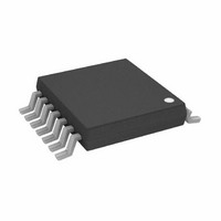
AD8303JRU Analog Devices Inc, AD8303JRU Datasheet - Page 10

AD8303JRU
Manufacturer Part Number
AD8303JRU
Description
IC DAC 12-BIT SERIAL 14-SOIC
Manufacturer
Analog Devices Inc
Datasheet
1.AD8303AR.pdf
(16 pages)
Specifications of AD8303JRU
Rohs Status
RoHS non-compliant
Settling Time
14µs
Number Of Bits
12
Data Interface
Serial, SPI™
Number Of Converters
2
Voltage Supply Source
Single Supply
Power Dissipation (max)
9.6mW
Operating Temperature
-40°C ~ 85°C
Mounting Type
Surface Mount
Package / Case
14-TSSOP
AD8303
DIGITAL INTERFACE
The AD8303 has a double-buffered serial data input. The
serial-input register is separate from the two DAC registers,
which allows preloading of a new data value into the serial
register without disturbing the present DAC values. A
functional block diagram of the digital section is shown in
Figure 27, while Table I contains the truth table for the control
logic inputs.
Three pins control the serial data input. Data at the Serial Data
Input (SDI) is clocked into the shift register on the rising edge
of CLK. Data is entered in MSB-first format. Twelve clock
pulses are required to load the 12-bit DAC value. If additional
bits are clocked into the shift register, for example when a C
sends two 8-bit bytes, the MSBs are ignored (Figure 28). The
CLK pin is only enabled when Chip Select (CS) is low. If only
one AD8303 is connected to a serial data bus, then CS can be
tied (hardwired) to ground.
Figure 28. Typical AD8303-Microprocessor Serial Data
Input Format
MSB
B15 B14 B13 B12 B11 B10 B9
D11–D0: 12-BIT DAC VALUE
X = DON'T CARE
THE MSB OF BYTE 1 IS THE FIRST BIT THAT IS LOADED INTO THE DAC
X
X
X
X
BYTE 1
D11 D10 D9
CLK
SDI
CS
B8
D8
LSB
B7
D7
Figure 27. AD8303 Digital Section Functional Block Diagram
en
MSB
B6
D6
B5
D5
D
AD8303
CLK
12-BIT SHIFT
REGISTER
B4
D4
BYTE 2
B3
D3
Q11–Q0
B2
D2
B1
D1
12
MSB RS
LSB
B0
D0
–10–
LDA
Separate Load pins (LDA and LDB) are provided to control the
flow of data from the shift register to the DAC registers. After
the new value is loaded in the serial-input register, it can be
asynchronously transferred to either DAC register by strobing
the appropriate Load pin (LDA or LDB). The Load pins are
level sensitive, so they should be returned high before any new
data is loaded into the serial-input register.
RESET (RS) AND MSB PINS
The RS pin forces both of the DAC registers to a known state,
based on the logic level on the MSB pin. If MSB is a logic zero,
then forcing RS low will set the DAC latches to all zeros and the
DAC output voltage will be zero volts. If MSB is a logic one, then
RS will force the DAC latches to one-half scale (800
DAC outputs will be 1.024 V. The half-scale reset is useful for
systems where the DAC output is referenced to a “false
ground” (see the Generating Bipolar Outputs with a Single
Supply section of this data sheet for more information).
The reset function is useful for setting the DAC outputs to zero
at power-up or after a power supply interruption. Test systems
and motor controllers are two of many applications which
benefit from powering up to a known state. The reset pulse can
be generated by the microprocessor’s power-on RESET signal,
by an output from the microprocessor (Figure 33), or by an
external resistor and capacitor (Figure 34).
RS and MSB have level-sensitive thresholds. The RS input
overrides other logic inputs (specifically, LDA and LDB).
However, LDA and LDB should be set high before RS goes
high. If LDA or LDB are kept low, then the contents of the shift
register will be transferred to the DAC register as soon as RS
goes high.
DAC REGISTER A
DAC REGISTER B
MSB
MSB
RESET LOAD
RESET LOAD
LDB
12
12
DAC A
DAC B
SHDN
V
V
OUTA
OUTB
H
) and the
REV. 0


