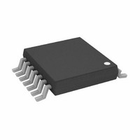
AD8303JRU Analog Devices Inc, AD8303JRU Datasheet - Page 4

AD8303JRU
Manufacturer Part Number
AD8303JRU
Description
IC DAC 12-BIT SERIAL 14-SOIC
Manufacturer
Analog Devices Inc
Datasheet
1.AD8303AR.pdf
(16 pages)
Specifications of AD8303JRU
Rohs Status
RoHS non-compliant
Settling Time
14µs
Number Of Bits
12
Data Interface
Serial, SPI™
Number Of Converters
2
Voltage Supply Source
Single Supply
Power Dissipation (max)
9.6mW
Operating Temperature
-40°C ~ 85°C
Mounting Type
Surface Mount
Package / Case
14-TSSOP
AD8303
ABSOLUTE MAXIMUM RATINGS*
V
Logic Inputs to GND . . . . . . . . . . . . . . . . . . . . . . –0.3 V, +8 V
V
I
Package Power Dissipation . . . . . . . . . . . . . . . (T
Thermal Resistance
Maximum Junction Temperature (T
Operating Temperature Range . . . . . . . . . . . . –40 C to +85 C
Storage Temperature Range . . . . . . . . . . . . . –65 C to +150 C
Lead Temperature (Soldering, 10 secs) . . . . . . . . . . . . .+300 C
*Stress above those listed under “Absolute Maximum Ratings” may cause perma-
CAUTION
ESD (electrostatic discharge) sensitive device. Electrostatic charges as high as 4000 V readily
accumulate on the human body and test equipment and can discharge without detection.
Although the AD8303 features proprietary ESD protection circuitry, permanent damage may
occur on devices subjected to high energy electrostatic discharges. Therefore, proper ESD
precautions are recommended to avoid performance degradation or loss of functionality.
nent damage to the device. This is a stress rating only and functional operation of
the device at these or any other conditions above those indicated in the operational
sections of this specification is not implied. Exposure to absolute maximum rating
conditions for extended periods may affect device reliability.
OUT
DD
OUT
14-Pin Plastic DIP Package (N-14) . . . . . . . . . . . . 103 C/W
14-Lead SOIC Package (R-14) . . . . . . . . . . . . . . . . 158 C/W
to GND . . . . . . . . . . . . . . . . . . . . . . . . . . . . . –0.3 V, +8 V
Short Circuit to GND . . . . . . . . . . . . . . . . . . . . . . 50 mA
to GND . . . . . . . . . . . . . . . . . . . . . . –0.3 V, V
JA
V
LDA, B
LDA, B
OUT
CLK
CLK
SDI
SDI
CS
RS
FS
ZS
t
LD1
D11
J MAX
t
CSS
D10
) . . . . . . . . . . . 150 C
SHDN
D9
t
CL
I
DD
J MAX
t
DS
Figure 3. Timing Diagrams
D8
DD
–T
t
DH
+ 0.3 V
D7
A
t
)/
CH
JA
D6
–4–
a.
b.
Model
AD8303AN
AD8303AR
The AD8303 contains 700 transistors. The die size measures 70 mil
D5
t
LDW
D4
t
t
SDR
S
D3
DNL Range
0.75 –40 C to +85 C 14-Pin P-DIP N-14
0.75 –40 C to +85 C 14-Lead SOIC R-14
D2
ERROR BAND
Temperature
ORDERING GUIDE
1 LSB
D1
t
CSH
D0
t
LD2
t
t
RS
S
WARNING!
Package
Description
ESD SENSITIVE DEVICE
Package
Option
99 mil.
REV. 0


