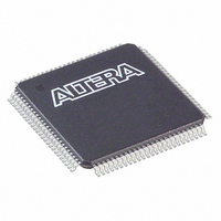
EPM570T100C3N Altera, EPM570T100C3N Datasheet - Page 53

EPM570T100C3N
Manufacturer Part Number
EPM570T100C3N
Description
IC MAX II CPLD 570 LE 100-TQFP
Manufacturer
Altera
Series
MAX® IIr
Specifications of EPM570T100C3N
Programmable Type
In System Programmable
Delay Time Tpd(1) Max
5.4ns
Voltage Supply - Internal
2.5V, 3.3V
Number Of Logic Elements/blocks
570
Number Of Macrocells
440
Number Of I /o
76
Operating Temperature
0°C ~ 85°C
Mounting Type
Surface Mount
Package / Case
100-TQFP, 100-VQFP
Voltage
2.5V, 3.3V
Memory Type
FLASH
Number Of Logic Elements/cells
570
Family Name
MAX II
# Macrocells
440
Frequency (max)
3.01205GHz
Propagation Delay Time
5.4ns
Number Of Logic Blocks/elements
57
# I/os (max)
76
Operating Supply Voltage (typ)
2.5/3.3V
In System Programmable
Yes
Operating Supply Voltage (min)
2.375V
Operating Supply Voltage (max)
3.6V
Operating Temp Range
0C to 85C
Operating Temperature Classification
Commercial
Mounting
Surface Mount
Pin Count
100
Package Type
TQFP
Lead Free Status / RoHS Status
Lead free / RoHS Compliant
Features
-
Lead Free Status / Rohs Status
Compliant
Other names
544-1315
EPM570T100C3N
EPM570T100C3N
Available stocks
Company
Part Number
Manufacturer
Quantity
Price
Part Number:
EPM570T100C3N
Manufacturer:
ALTERA/阿尔特拉
Quantity:
20 000
Chapter 4: Hot Socketing and Power-On Reset in MAX II Devices
Hot Socketing Feature Implementation in MAX II Devices
Figure 4–1. Hot Socketing Circuit Block Diagram for MAX II Devices
© October 2008 Altera Corporation
f
1
Make sure that the V
SRAM download has completed.
Each I/O and clock pin has the circuitry shown in
The POR circuit monitors V
until the device has completed its flash memory configuration of the SRAM logic. The
weak pull-up resistor (R) from the I/O pin to V
keep the I/O pins from floating. The 3.3-V tolerance control circuit permits the I/O
pins to be driven by 3.3 V before V
I/O pins from driving out when the device is not fully powered or operational. The
hot socket circuit prevents I/O pins from internally powering V
driven by external signals before the device is powered.
For information about 5.0-V tolerance, refer to the
Voltage Systems
Figure 4–2
This design ensures that the output buffers do not drive when V
V
voltage spikes during hot insertion. The V
tolerant circuit capacitance.
Resistor
Pull-Up
CCINT
Weak
PAD
or if the I/O pad voltage is higher than V
shows a transistor-level cross section of the MAX II device I/O buffers.
chapter in the MAX II Device Handbook.
V
CCINT
CCIO
is within the recommended operating range even though
CCINT
and V
Input Buffer
to Logic Array
CCIO
Tolerance
Voltage
Control
CCIO
and/or V
voltage levels and keeps I/O pins tri-stated
PAD
Output Enable
leakage current charges the 3.3-V
CCIO
CCIO
CCINT
Using MAX II Devices in Multi-
Figure
. This also applies for sudden
is enabled during download to
Hot Socket
are powered, and it prevents the
Power On
Monitor
Reset
4–1.
CCIO
CCIO
is powered before
and V
MAX II Device Handbook
CCINT
when
4–3


