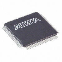
EPM570T100C3N Altera, EPM570T100C3N Datasheet - Page 62

EPM570T100C3N
Manufacturer Part Number
EPM570T100C3N
Description
IC MAX II CPLD 570 LE 100-TQFP
Manufacturer
Altera
Series
MAX® IIr
Specifications of EPM570T100C3N
Programmable Type
In System Programmable
Delay Time Tpd(1) Max
5.4ns
Voltage Supply - Internal
2.5V, 3.3V
Number Of Logic Elements/blocks
570
Number Of Macrocells
440
Number Of I /o
76
Operating Temperature
0°C ~ 85°C
Mounting Type
Surface Mount
Package / Case
100-TQFP, 100-VQFP
Voltage
2.5V, 3.3V
Memory Type
FLASH
Number Of Logic Elements/cells
570
Family Name
MAX II
# Macrocells
440
Frequency (max)
3.01205GHz
Propagation Delay Time
5.4ns
Number Of Logic Blocks/elements
57
# I/os (max)
76
Operating Supply Voltage (typ)
2.5/3.3V
In System Programmable
Yes
Operating Supply Voltage (min)
2.375V
Operating Supply Voltage (max)
3.6V
Operating Temp Range
0C to 85C
Operating Temperature Classification
Commercial
Mounting
Surface Mount
Pin Count
100
Package Type
TQFP
Lead Free Status / RoHS Status
Lead free / RoHS Compliant
Features
-
Lead Free Status / Rohs Status
Compliant
Other names
544-1315
EPM570T100C3N
EPM570T100C3N
Available stocks
Company
Part Number
Manufacturer
Quantity
Price
Part Number:
EPM570T100C3N
Manufacturer:
ALTERA/阿尔特拉
Quantity:
20 000
5–4
Table 5–4. MAX II Device DC Electrical Characteristics
MAX II Device Handbook
I
C
C
Notes to
(1) Typical values are for T
(2) This value is specified for normal device operation. The value may vary during power-up. This applies for all V
(3) V
(4) Commercial temperature ranges from 0°C to 85°C with maximum current at 85°C.
(5) Industrial temperature ranges from –40°C to 100°C with maximum current at 100°C.
(6) This value applies to commercial and industrial range devices. For extended temperature range devices, the V
(7) The TCK input is susceptible to high pulse glitches when the input signal fall time is greater than 200 ns for all I/O standards.
(8) This is a peak current value with a maximum duration of t
(9) Pin pull-up resistance values will lower if an external source drives the pin higher than V
PULLUP
IO
GCLK
Symbol
1.8, and 1.5 V).
300 mV for V
I
= ground, no load, no toggling inputs.
Table
5–4:
I/O pin pull-up resistor
current when I/O is
unprogrammed
Input capacitance for
user I/O pin
Input capacitance for
dual-purpose
GCLK/user I/O pin
CC IO
= 3.3 V and 120 mV for V
Parameter
A
= 25°C, V
CCINT
= 3.3 or 2.5 V, and V
C CIO
= 2.5 V.
Conditions
—
—
—
CONFIG
CC IO
(Note 1)
= 1.5 V, 1.8 V, 2.5 V, or 3.3 V.
time.
(Part 2 of 2)
Minimum
—
—
—
C CIO
.
Typical
Chapter 5: DC and Switching Characteristics
—
—
—
Maximum
© August 2009 Altera Corporation
S CHM ITT
300
C CIO
8
8
settings (3.3, 2.5,
typical value is
Operating Conditions
Unit
µA
pF
pF


