CY7C372I-100JC Cypress Semiconductor Corp, CY7C372I-100JC Datasheet
CY7C372I-100JC
Specifications of CY7C372I-100JC
Available stocks


Related parts for CY7C372I-100JC


CY7C372I-100JC Summary of contents
Page 1
... F often allows users to change existing logic designs while si- multaneously fixing pinout assignments. The 64 macrocells in the CY7C372i are divided between four logic blocks. Each logic block includes 16 macrocells product term array, and an intelligent product term al- locator. ...
Page 2
... PIM regardless of its configuration. Programmable Interconnect Matrix The Programmable Interconnect Matrix (PIM) connects the four logic blocks on the CY7C372i to the inputs and to each other. All inputs (including feedbacks) travel through the PIM. There is no speed penalty incurred by signals traversing the PIM ...
Page 3
... V Design Tools Development software for the CY7C372i is available from Cypress’s Warp™, Warp Professional™, and Warp Enter- prise™ software packages. Please refer to the data sheets on these products for more details. Cypress also actively sup- ports almost all third-party design tools ...
Page 4
... V = Min 0. Min 2. Max Max. CC Test Conditions MHz 5. MHz IN Test Conditions MHz CY7C372i Min. Typ. Max. [5] 2.4 2.4 [5, 6] [5, 6] [5] 2.0 –0.5 –10 , Output –50 CC [6] 0 –70 –125 –30 –160 Com’l/Ind. 75 Com’l “L” –66 45 Military 75 +75 –75 +500 Min ...
Page 5
... JIG AND SCOPE (b) 3.0V 2.08V(com'l) GND 2.13V(mil) < Output Waveform Measurement Level V OH 0. 0.5V (d) Test Waveforms measured with 35-pF AC Test Load. EA CY7C372i Max. 100 170 (com'l) 236 (mil) 7c372i–3 ALL INPUT PULSES 90% 90% 10% 10% < (c) 7c372i– Unit Cycles ...
Page 6
... All AC parameters are measured with 16 outputs switching and 35-pF AC Test Load. 15. This specification is intended to guarantee interface compatibility of the other members of the CY7C370i family with the CY7C372i. This specification is met for the devices operating at the same ambient temperature and at the same power supply voltage. ...
Page 7
... OUTPUT Registered Output INPUT CLOCK REGISTERED OUTPUT CLOCK Document #: 38-03033 Rev (continued) 7C372i-125 Min. Max. 8 125 + t ), 1/( [9] 10 [9] 12 [1] 16 [9] 10 [9] 12 [1] 16 500 CY7C372i 7C372i-83 7C372i-66 7C372i-100 7C372iL-83 7C372iL-66 Min. Max. Min. Max. Min 100 83.3 66 500 500 500 Max. ...
Page 8
... Latched Output INPUT LATCH ENABLE LATCHED OUTPUT Registered Input REGISTERED INPUT INPUT REGISTER CLOCK COMBINATORIAL OUTPUT CLOCK Clock to Clock REGISTERED INPUT INPUT REGISTER CLOCK OUTPUT REGISTER CLOCK Document #: 38-03033 Rev PDL ICS CY7C372i ICO SCS 7c372i–7 7c372i–8 7c372i–9 Page ...
Page 9
... Latched Input and Output LATCHED INPUT LATCHED OUTPUT INPUT LATCH ENABLE OUTPUT LATCH ENABLE LATCH ENABLE Asynchronous Reset INPUT REGISTERED OUTPUT CLOCK Asynchronous Preset INPUT REGISTERED OUTPUT CLOCK Document #: 38-03033 Rev ICOL t ICS CY7C372i t PDLL 7c372i– 7c372i– 7c372i–13 Page ...
Page 10
... Switching Waveforms (continued) Output Enable/Disable INPUT OUTPUTS Ordering Information Speed (MHz) Ordering Code 125 CY7C372i-125JC 100 CY7C372i-100JC CY7C372i-100JI 83 CY7C372i-83JC CY7C372i-83JI CY7C372i-83YMB 83 CY7C372iL-83JC 66 CY7C372i-66JC CY7C372i-66JI CY7C372i-66YMB 66 CY7C372iL-66JC MILITARY SPECIFICATIONS Group A Subgroup Testing DC Characteristics Parameter Subgroups ISR, UltraLogic, F 370, F 370i, Warp, Warp Professional, and Warp Enterprise, are trademarks of Cypress Semiconductor ...
Page 11
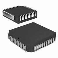
... The inclusion of Cypress Semiconductor products in life-support systems application implies that the manufacturer assumes all risk of such use and in doing so indemnifies Cypress Semiconductor against all charges. 44-Lead Plastic Leaded Chip Carrier J67 44-P in Ceramic Leaded Chip Carrier Y67 CY7C372i 51-85003-A Page ...
Page 12
... Document Title: CY7C372i UltraLogic™ 64-Macrocell Flash CPLD Document Number: 38-03033 Issue REV. ECN NO. Date ** 106378 06/18/01 Document #: 38-03033 Rev. ** Orig. of Change Decsription of Change SZV Change from Spec# 38-00498 to 38-03033 CY7C372i Page ...