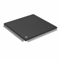
ADSP-BF532SBSTZ400 Analog Devices Inc, ADSP-BF532SBSTZ400 Datasheet - Page 38

ADSP-BF532SBSTZ400
Manufacturer Part Number
ADSP-BF532SBSTZ400
Description
IC DSP CTLR 16BIT 400MHZ 176LQFP
Manufacturer
Analog Devices Inc
Series
Blackfin®r
Type
Fixed Pointr
Datasheet
1.ADSP-BF531SBSTZ400.pdf
(12 pages)
Specifications of ADSP-BF532SBSTZ400
Interface
SPI, SSP, UART
Clock Rate
400MHz
Non-volatile Memory
ROM (1 kB)
On-chip Ram
84kB
Voltage - I/o
1.8V, 2.5V, 3.3V
Voltage - Core
1.20V
Operating Temperature
-40°C ~ 85°C
Mounting Type
Surface Mount
Package / Case
176-LQFP
No. Of Bits
16 Bit
Frequency
400MHz
Supply Voltage
1.2V
Embedded Interface Type
PPI, SPI, UART
No. Of I/o's
16
Supply Voltage Range
0.8V To 1.45V, 1.75V To 3.6V
Lead Free Status / RoHS Status
Lead free / RoHS Compliant
For Use With
ADZS-BF533-EZLITE - KIT W/BOARD EVAL FOR ADSP-BF533
Lead Free Status / RoHS Status
Lead free / RoHS Compliant, Lead free / RoHS Compliant
Available stocks
Company
Part Number
Manufacturer
Quantity
Price
Company:
Part Number:
ADSP-BF532SBSTZ400
Manufacturer:
TOSHIBA
Quantity:
101
Company:
Part Number:
ADSP-BF532SBSTZ400
Manufacturer:
Analog Devices Inc
Quantity:
10 000
Part Number:
ADSP-BF532SBSTZ400
Manufacturer:
ADI/亚德诺
Quantity:
20 000
ADSP-BF531/BF532/BF533
67.
DESCRIPTION:
When an access to a GPIO / Flag IO System MMR (any register with a PORTFIO_ or FIO_ prefix) is followed by another System MMR access
that is not in the GPIO / Flag IO block, the GPIO's input driver can spuriously become active for a moment. As a result, the output values
held in the Port F latch may clear erroneously, causing unwanted transitions in pin state on the output pins.
Only certain combinations of MMR accesses can trigger this failure, and they vary with the type of GPIO register access (i.e., write, read,
aborted read). Some failures may occur very rarely and are unlikely to be detected during system evaluation. Because of this, it must be
assumed that any MMR combination where the address bits 4, 5, or 6 differ between the GPIO register and the subsequent MMR can
generate this failure. Furthermore, the two MMR accesses need not occur in consecutive instructions for the problem to occur. The
accesses can be separated by an unlimited number of cycles/instructions.
Accesses to multiple GPIO/FIO registers do not disturb each other, and GPIO flag pins configured as inputs are not impacted.
WORKAROUND:
Every sequence of accesses to GPIO registers must be terminated by a safe register read. A "safe register" is defined as any non-GPIO
system MMR that has the same address bits 4, 5, and 6 as the last accessed GPIO register. The workaround must ensure this rule is not
violated by non-linear program flow, such as conditional jumps or interrupts. As a welcomed side-effect, aborted GPIO MMR reads are
avoided entirely. For example, the following sequence is safe:
Note that address bits 4, 5 and 6 of SYSCR and PORTFIO_CLEAR are 000. Therefore, a SYSCR read safely resolves the critical situation
introduced by the PORTFIO_CLEAR access.
The following is a comprehensive list of safe registers for each GPIO/FIO register.
SPECIAL TOOLS IMPACT:
In VisualDSP++ 4.5 (February 2007 Update), the compiler inserted a dummy read of CHIPID. However, since the dummy read address
varies (and since interrupts must be disabled), the workaround was replaced in VisualDSP++ 4.5 (June 2007 Update) by header
05000311.h, which defines macros for doing this under user control instead of compiler control. See the header file for more details.
APPLIES TO REVISION(S):
0.3, 0.4, 0.5
05000311 - Erroneous Flag (GPIO) Pin Operations under Specific Sequences:
If the last GPIO access was to...
PORTFIO/_CLEAR/_SET/_TOGGLE (FIO_FLAG_D/C/S/T)
PORTFIO_MASKA/_CLEAR/_SET/_TOGGLE (FIO_MASKA_D/C/S/T)
PORTFIO_MASKB/_CLEAR/_SET/_TOGGLE (FIO_MASKB_D/C/S/T)
PORTFIO_DIR/POLAR/EDGE/BOTH (FIO_DIR/POLAR/EDGE/BOTH)
PORTFIO_INEN (FIO_INEN)
P5.H = hi(PORTFIO);
P4.H = hi(SYSCR);
cli R7;
nop; nop; nop;
/* any GPIO sequence */
R6 = w[P5](z);
R5 = w[P5+PORTFIO_MASKA-PORTFIO](z);
R6 = R5 & R6;
w[P5+PORTFIO_CLEAR-PORTFIO] = R6;
R5 = w[P4](z);
sti R7;
/* avoid interrupts */
/* three cycles after CLI before 1st FIO read access
/* restore interrupts */
P5.L = lo(PORTFIO);
P4.L = lo(SYSCR);
NR003532D | Page 38 of 45 | July 2008
/* last GPIO access to PORTFIO_CLEAR (0xFFC00704) */
/* dummy read from SYSCR (0xFFC00104) */
/* PORTFIO_MASKA_D read */
/* PORTFIO is the same as FIO_FLAG_D */
Then the "safe registers" are...
SYSCR, PPI_STATUS, or SPI_STAT
UART_SCR, TIMER1_CONFIG, or EBIU_SDSTAT
UART_GCTL, TIMER2_CONFIG, or DMA0_IRQ_STATUS
SPORT0_STAT, SPORT1_STAT, or DMA0_CURR_X_COUNT
TIMER_ENABLE, TIMER_STATUS, or DMA1_CONFIG
Silicon Anomaly List
*/


