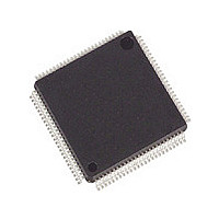
ADSP-2184NBST-320 Analog Devices Inc, ADSP-2184NBST-320 Datasheet - Page 11

ADSP-2184NBST-320
Manufacturer Part Number
ADSP-2184NBST-320
Description
IC DSP CONTROLLER 16BIT 100LQFP
Manufacturer
Analog Devices Inc
Series
ADSP-21xxr
Type
Fixed Pointr
Datasheet
1.ADSP-2185NKSTZ-320.pdf
(48 pages)
Specifications of ADSP-2184NBST-320
Rohs Status
RoHS non-compliant
Interface
Host Interface, Serial Port
Clock Rate
80MHz
Non-volatile Memory
External
On-chip Ram
20kB
Voltage - I/o
3.30V
Voltage - Core
1.90V
Operating Temperature
-40°C ~ 85°C
Mounting Type
Surface Mount
Package / Case
100-LQFP
Device Core Size
16b
Architecture
Enhanced Harvard
Format
Fixed Point
Clock Freq (max)
80MHz
Mips
80
Device Input Clock Speed
80MHz
Ram Size
20KB
Program Memory Size
Not RequiredKB
Operating Supply Voltage (typ)
2.5/3.3V
Operating Supply Voltage (min)
1.8V
Operating Supply Voltage (max)
2/3.6V
Operating Temp Range
-40C to 85C
Operating Temperature Classification
Industrial
Mounting
Surface Mount
Pin Count
100
Package Type
LQFP
Lead Free Status / Rohs Status
Not Compliant
Available stocks
Company
Part Number
Manufacturer
Quantity
Price
Company:
Part Number:
ADSP-2184NBST-320
Manufacturer:
SAMSUNG
Quantity:
958
Program Memory (Host Mode) allows access to all internal
memory. External overlay access is limited by a single external
address line (A0). External program execution is not available in
host mode due to a restricted data bus that is only 16 bits wide.
Table 4. PMOVLAY Bits
Data Memory
Data Memory (Full Memory Mode) is a 16-bit-wide space used
for the storage of data variables and for memory-mapped con-
trol registers. The ADSP-218xN series has up to 56K words of
Data Memory RAM on-chip. Part of this space is used by 32
memory-mapped registers. Support also exists for up to two 8K
external memory overlay spaces through the external data bus.
Table 5. DMOVLAY Bits
Memory-Mapped Registers (New to the ADSP-218xM and
N series)
ADSP-218xN series members have three memory-mapped reg-
isters that differ from other ADSP-21xx Family DSPs. The slight
modifications to these registers (Wait State Control, Program-
mable Flag and Composite Select Control, and System Control)
provide the ADSP-218xN’s wait state and BMS control features.
Default bit values at reset are shown; if no value is shown, the bit
is undefined at reset. Reserved bits are shown on a grey field.
These bits should always be written with zeros.
Processor
ADSP-2184N
ADSP-2185N
ADSP-2186N
ADSP-2187N
ADSP-2188N
ADSP-2189N
All Processors
All Processors
Processor
ADSP-2184N
ADSP-2185N
ADSP-2186N
ADSP-2187N
ADSP-2188N
ADSP-2189N
All Processors
All Processors
PMOVLAY
No Internal Overlay
Region
0
No Internal Overlay
Region
0, 4, 5
0, 4, 5, 6, 7
0, 4, 5
1
2
DMOVLAY
No Internal Overlay Region
0
No Internal Overlay Region
0, 4, 5
0, 4, 5, 6, 7, 8
0, 4, 5, 6, 7
1
2
Memory
Not Applicable
Internal Overlay
Not Applicable
Internal Overlay
Internal Overlay
Internal Overlay
External Overlay 1
External Overlay 2
Memory
Not Applicable
Internal Overlay
Not Applicable
Internal Overlay
Internal Overlay
Internal Overlay
External Overlay 1
External Overlay 2
Rev. A | Page 11 of 48 | August 2006
A13
Not Applicable
Not Applicable
Not Applicable
Not Applicable
Not Applicable
Not Applicable
0
1
All internal accesses complete in one cycle. Accesses to external
memory are timed using the wait states specified by the DWAIT
register and the wait state mode bit.
Data Memory (Host Mode) allows access to all internal mem-
ory. External overlay access is limited by a single external
address line (A0).
I/O Space (Full Memory Mode)
ADSP-218xN series members support an additional external
memory space called I/O space. This space is designed to sup-
port simple connections to peripherals (such as data converters
and external registers) or to bus interface ASIC data registers.
I/O space supports 2048 locations of 16-bit wide data. The lower
eleven bits of the external address bus are used; the upper three
bits are undefined.
Two instructions were added to the core ADSP-2100 Family
instruction set to read from and write to I/O memory space. The
I/O space also has four dedicated three-bit wait state registers,
A13
Not Applicable
Not Applicable
Not Applicable
Not Applicable
Not Applicable
Not Applicable
0
1
A12–0
Not Applicable
Not Applicable
Not Applicable
Not Applicable
Not Applicable
Not Applicable
13 LSBs of Address Between 0x2000 and 0x3FFF
13 LSBs of Address Between 0x2000 and 0x3FFF
A12–0
Not Applicable
Not Applicable
Not Applicable
Not Applicable
Not Applicable
Not Applicable
13 LSBs of Address
Between 0x0000 and
0x1FFF
13 LSBs of Address
Between 0x0000 and
0x1FFF
ADSP-218xN


