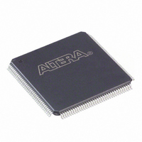
EP1C3T144C6 Altera, EP1C3T144C6 Datasheet - Page 53

EP1C3T144C6
Manufacturer Part Number
EP1C3T144C6
Description
IC CYCLONE FPGA 2910 LE 144-TQFP
Manufacturer
Altera
Series
Cyclone®r
Datasheet
1.EP1C3T144C8.pdf
(106 pages)
Specifications of EP1C3T144C6
Number Of Logic Elements/cells
2910
Number Of Labs/clbs
291
Total Ram Bits
59904
Number Of I /o
104
Voltage - Supply
1.425 V ~ 1.575 V
Mounting Type
Surface Mount
Operating Temperature
0°C ~ 85°C
Package / Case
144-TQFP, 144-VQFP
Lead Free Status / RoHS Status
Contains lead / RoHS non-compliant
Number Of Gates
-
Other names
544-1050
Available stocks
Company
Part Number
Manufacturer
Quantity
Price
Company:
Part Number:
EP1C3T144C6
Manufacturer:
ALTERA
Quantity:
70
Company:
Part Number:
EP1C3T144C6
Manufacturer:
ALTERA
Quantity:
250
Part Number:
EP1C3T144C6
Manufacturer:
ALTERA/阿尔特拉
Quantity:
20 000
Company:
Part Number:
EP1C3T144C6N
Manufacturer:
ALTERA
Quantity:
250
Part Number:
EP1C3T144C6N
Manufacturer:
ALTERA
Quantity:
20 000
Figure 2–33. Cyclone Device DQ and DQS Groups in ×8 Mode
Note to
(1)
Altera Corporation
May 2008
Each DQ group consists of one DQS pin, eight DQ pins, and one DM pin.
Figure
Top, Bottom, Left, or Right I/O Bank
2–33:
output pins (nSTATUS and CONF_DONE) and all the JTAG pins in I/O
bank 3 must operate at 2.5 V because the V
I/O banks 1, 2, 3, and 4 support DQS signals with DQ bus modes of × 8.
For × 8 mode, there are up to eight groups of programmable DQS and DQ
pins, I/O banks 1, 2, 3, and 4 each have two groups in the 324-pin and
400-pin FineLine BGA packages. Each group consists of one DQS pin, a
set of eight DQ pins, and one DM pin (see
drives the set of eight DQ pins within that group.
Table 2–10
EP1C3
EP1C4
Table 2–10. DQ Pin Groups (Part 1 of 2)
Device
DQ Pins
shows the number of DQ pin groups per device.
100-pin TQFP
144-pin TQFP
324-pin FineLine BGA
400-pin FineLine BGA
DQS Pin
Package
(1)
Note (1)
Number of × 8 DQ
Pin Groups
Figure
CCIO
3
4
8
8
level of SSTL-2 is 2.5 V.
2–33). Each DQS pin
DM Pin
Total DQ Pin
I/O Structure
Count
Preliminary
24
32
64
64
2–47


