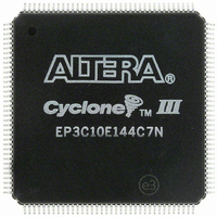
EP3C10E144C7N Altera, EP3C10E144C7N Datasheet - Page 25

EP3C10E144C7N
Manufacturer Part Number
EP3C10E144C7N
Description
IC CYCLONE III FPGA 10K 144-EQFP
Manufacturer
Altera
Series
Cyclone® IIIr
Datasheets
1.EP3C5F256C8N.pdf
(5 pages)
2.EP3C5F256C8N.pdf
(34 pages)
3.EP3C5F256C8N.pdf
(66 pages)
4.EP3C5F256C8N.pdf
(14 pages)
5.EP3C5F256C8N.pdf
(76 pages)
Specifications of EP3C10E144C7N
Number Of Logic Elements/cells
10320
Number Of Labs/clbs
645
Total Ram Bits
423936
Number Of I /o
94
Voltage - Supply
1.15 V ~ 1.25 V
Mounting Type
Surface Mount
Operating Temperature
0°C ~ 85°C
Package / Case
144-EQFP
For Use With
544-2601 - KIT DEV CYCLONE III LS EP3CLS200544-2411 - KIT DEV NIOS II CYCLONE III ED.
Lead Free Status / RoHS Status
Lead free / RoHS Compliant
Number Of Gates
-
Other names
544-2425
EP3C10E144C7N
EP3C10E144C7N
Available stocks
Company
Part Number
Manufacturer
Quantity
Price
Company:
Part Number:
EP3C10E144C7N
Manufacturer:
ALTERA
Quantity:
364
Part Number:
EP3C10E144C7N
Manufacturer:
ALTERA
Quantity:
20 000
Board Design Considerations
Unused JTAG Pins Connection
© November 2008 Altera Corporation
In a JTAG chain containing devices with different V
V
must maintain a maximum AC voltage of 4.1 V. To prevent voltage overshoot when
using V
a 2.5 V supply from V
power up the download cable's V
download cables do not support a target supply voltage of 1.2 V. You only need one
level shifter at the end of the chain with this device arrangement. If this arrangement
is not possible, you have to add more level shifters into the chain.
JTAG chain that contains devices with different V
Figure 2. Devices with Different VCCIO in a JTAG Chain
JTAG Signal Buffering
The JTAG signal integrity determines the need to buffer a JTAG chain. Pay particular
attention to the TCK signal because it is the JTAG clock and is the fastest switching
signal compared to the other JTAG signals. Altera recommends buffering the signals
at the connector because cables and board connectors tend to act as poor transmission
lines and introduce noise to the signals. After this initial buffer at the connector, add
buffers as the chain gets longer or whenever the signals must cross a board connector.
At any given time, when a cable must drive three or more devices, buffer the signal at
the cable connector to prevent signal deterioration. The decision to buffer the signal
also depends on the board layout, loads, connectors, jumpers, and switches on the
board. Anything added to the board that affects the inductance or capacitance of the
JTAG signals increases the likelihood of a buffer being added to the chain.
For the TCK and TMS signals that drive in parallel, each buffer should drive no greater
than eight loads. If jumper or switches are added to the path, decrease the number of
loads.
If you are not using the JTAG interface, make sure the JTAG pins on the Cyclone III
device are not left floating and are connected to a stable level. Because JTAG
configuration takes precedence over all other configuration methods, these pins
should not be left floating or toggling during configuration.
CCIO
level should drive the devices with the same or lower V
CCIO
of 2.5 V, 3.0 V, or 3.3 V, you must power up the download cable's V
Download
Power TDI from
2.5 V VCCA
header
Shift TDO to level
acceptable by tester
if necessary
cable
CCA
TDI
TDO
. When using device V
VCCIO
Shifter
Level
3.3 V
CC
with the supply from V
Must never exceed
overshoot of 4.1 V
VCCIO
VCCIO
1.5 V
CCIO
3.0 V
CCIO
CCIO
of 1.2 V, 1.5 V, or 1.8 V, you can
.
, the devices with a higher
CCIO
CCIO
VCCIO
VCCIO
2.5 V
1.8 V
. However, Altera
level. All I/O inputs
Figure 2
shows the
CC
Page 25
with


