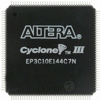
EP3C10E144C7N Altera, EP3C10E144C7N Datasheet - Page 28

EP3C10E144C7N
Manufacturer Part Number
EP3C10E144C7N
Description
IC CYCLONE III FPGA 10K 144-EQFP
Manufacturer
Altera
Series
Cyclone® IIIr
Datasheets
1.EP3C5F256C8N.pdf
(5 pages)
2.EP3C5F256C8N.pdf
(34 pages)
3.EP3C5F256C8N.pdf
(66 pages)
4.EP3C5F256C8N.pdf
(14 pages)
5.EP3C5F256C8N.pdf
(76 pages)
Specifications of EP3C10E144C7N
Number Of Logic Elements/cells
10320
Number Of Labs/clbs
645
Total Ram Bits
423936
Number Of I /o
94
Voltage - Supply
1.15 V ~ 1.25 V
Mounting Type
Surface Mount
Operating Temperature
0°C ~ 85°C
Package / Case
144-EQFP
For Use With
544-2601 - KIT DEV CYCLONE III LS EP3CLS200544-2411 - KIT DEV NIOS II CYCLONE III ED.
Lead Free Status / RoHS Status
Lead free / RoHS Compliant
Number Of Gates
-
Other names
544-2425
EP3C10E144C7N
EP3C10E144C7N
Available stocks
Company
Part Number
Manufacturer
Quantity
Price
Company:
Part Number:
EP3C10E144C7N
Manufacturer:
ALTERA
Quantity:
364
Part Number:
EP3C10E144C7N
Manufacturer:
ALTERA
Quantity:
20 000
Page 28
Design and Compilation
Design Entry
f
f
Flash Pins and other Pin Connections
For information on the flash pin connections for the AP configurations scheme, refer
to the
Handbook.
Flash for AP
In the AP configuration scheme, the commodity parallel flash is used as configuration
memory. The AP configuration controller in Cyclone III devices is designed to
interface with the Intel StrataFlash
Unlike the EPCS devices, the P30 and P33 flash families supported in the AP
configuration scheme is designed to interface with microprocessors. By configuring
from an industry standard microprocessor flash which allows access to flash after it is
in user mode, the AP configuration scheme allows you to combine configuration data
and user data (microprocessor boot code) on the same flash memory.
The Intel P30 and P33 flash families support a continuous synchronous burst read
mode at 40 MHz DCLK frequency for reading data from the flash. You must refer to
the respective flash datasheets to check for the supported speed grades and package
options. For example, the Intel P30 and P33 families have only a single speed grade at
40 MHz; however, they do not support 40 MHz on the TSOP package. Therefore, the
P30 and P33 FBGA packages are supported for the AP configuration scheme, while
the TSOP package is not supported.
For more information about the active parallel configuration scheme and its
supported parallel flash, refer to the
volume 1 of the Cyclone III Device Handbook.
This section covers topics you should look into during the design process, which
includes design entry consideration and recommendation, power consideration,
information on the Cyclone III I/O pins and PLLs, timing consideration as well as
information on performing simulation on your design.
The Quartus II software allows you to create your design through schematic/block
diagram or hardware description language (HDL) coding. The commonly used HDL
formats supported are Verilog and VHDL. For simple designs, using schematic or
block diagrams make your task of creating the design easier. However, for more
complex designs, for example designs with state machines, using HDL coding gives
you the flexibility you need, and in some cases, makes your design more efficient.
If you use HDL as the design entry for your design, pay attention to the coding style.
HDL coding has a significant effect on the quality of results in terms of logic
utilization and performance that you achieve for your designs. Effective coding helps
the synthesis tool to perform better when synthesizing your design.
Configuring Cyclone III Devices
®
Embedded Memory (P30 and P33) flash families.
chapter in volume 1 of the Cyclone III Device
Configuring Cyclone III Devices
© November 2008 Altera Corporation
chapter in
Design and Compilation


