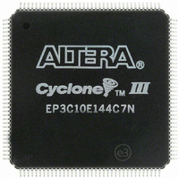
EP3C10E144C7N Altera, EP3C10E144C7N Datasheet - Page 61

EP3C10E144C7N
Manufacturer Part Number
EP3C10E144C7N
Description
IC CYCLONE III FPGA 10K 144-EQFP
Manufacturer
Altera
Series
Cyclone® IIIr
Datasheets
1.EP3C5F256C8N.pdf
(5 pages)
2.EP3C5F256C8N.pdf
(34 pages)
3.EP3C5F256C8N.pdf
(66 pages)
4.EP3C5F256C8N.pdf
(14 pages)
5.EP3C5F256C8N.pdf
(76 pages)
Specifications of EP3C10E144C7N
Number Of Logic Elements/cells
10320
Number Of Labs/clbs
645
Total Ram Bits
423936
Number Of I /o
94
Voltage - Supply
1.15 V ~ 1.25 V
Mounting Type
Surface Mount
Operating Temperature
0°C ~ 85°C
Package / Case
144-EQFP
For Use With
544-2601 - KIT DEV CYCLONE III LS EP3CLS200544-2411 - KIT DEV NIOS II CYCLONE III ED.
Lead Free Status / RoHS Status
Lead free / RoHS Compliant
Number Of Gates
-
Other names
544-2425
EP3C10E144C7N
EP3C10E144C7N
Available stocks
Company
Part Number
Manufacturer
Quantity
Price
Company:
Part Number:
EP3C10E144C7N
Manufacturer:
ALTERA
Quantity:
364
Part Number:
EP3C10E144C7N
Manufacturer:
ALTERA
Quantity:
20 000
Design Checklist
Design Checklist
© November 2008 Altera Corporation
Project Name:
Date:
“Device Selection” on page 1
“Early System Planning” on page 3
1
2
3
4
5
6
7
8
9
10
11
12
13
14
15
16
17
18
Done
Done
N/A
N/A
This checklist provides a summary of the guidelines described in this document. Use
the checklist to verify that you have followed the guidelines for each stage of your
design.
Estimate power consumption and heat dissipation with the Early Power Estimator
spreadsheet to plan the cooling solution and power supplies.
Reduce I/O power consumption with lower I/O capacitance, lower voltage I/O standards,
and resistively terminated I/O standards for high frequency signals.
Select suitable I/O standard (single-ended, voltage-referenced, or differential) for your
design.
Place I/O pins that share the same V
Select the configuration scheme based on the Cyclone III device package, the resources
available for the configuration, and the configuration time required by your system.
For AS, AP, and PS configuration schemes, you can select either fast or standard POR time.
For AS configuration scheme, make sure the selected EPCS device supports the
configuration bitstream file size for the selected Cyclone III device.
For AS configuration scheme, use SFL to reduce the effort to have separate programming
interface for your Cyclone III and EPCS device.
When using MAX II PFL for PS or FPP configuration scheme, or when using FPGA-based
PFL for AP configuration scheme, ensure that you select the appropriate flash device
according to the list of supported flash devices.
Use the compression feature to reduce the configuration file size for AS and PS
configuration schemes.
Use the Cyclone III PLL for frequency synthesis and clock management.
Ensure that the PLL input, output, and VCO frequency are within the specification in the
datasheet.
Cascade the PLLs to obtain the frequency you need, if the m, n, c counter or VCO frequency
does not allow you to obtain the desired frequency when one PLL is used.
Use the clock switchover feature of the PLL, if you need a backup input clock or to change
the input clock source in user mode.
Select the PLL compensation mode that best fits your design requirement.
Use the PLL reconfiguration feature, if you need to change the PLL settings on the fly in user
mode without reconfiguring the entire Cyclone III device.
Select a device based on the logic/memory/multiplier density, device features such as PLLs,
I/O pin count, package offering, and additional resources for debugging future development.
Consider vertical device migration requirements. Consider availability of speed grades.
Ensure sufficient timing margin if you plan to use a lower speed grade device in the future.
CCIO
and V
REF
in the same I/O bank.
Page 61


