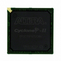
EP2C70F672C8N Altera, EP2C70F672C8N Datasheet - Page 157

EP2C70F672C8N
Manufacturer Part Number
EP2C70F672C8N
Description
IC CYCLONE II FPGA 70K 672-FBGA
Manufacturer
Altera
Series
Cyclone® IIr
Datasheet
1.EP2C5T144C8N.pdf
(168 pages)
Specifications of EP2C70F672C8N
Number Of Logic Elements/cells
68416
Number Of Labs/clbs
4276
Total Ram Bits
1152000
Number Of I /o
422
Voltage - Supply
1.15 V ~ 1.25 V
Mounting Type
Surface Mount
Operating Temperature
0°C ~ 85°C
Package / Case
672-FBGA
No. Of Logic Blocks
4276
Family Type
Cyclone II
No. Of I/o's
422
I/o Supply Voltage
3.3V
Operating Frequency Max
320MHz
Operating Temperature Range
0°C To +85°C
Rohs Compliant
Yes
Family Name
Cyclone® II
Number Of Logic Blocks/elements
68416
# I/os (max)
422
Frequency (max)
402.58MHz
Process Technology
90nm
Operating Supply Voltage (typ)
1.2V
Logic Cells
68416
Ram Bits
1152000
Operating Supply Voltage (min)
1.15V
Operating Supply Voltage (max)
1.25V
Operating Temp Range
0C to 85C
Operating Temperature Classification
Commercial
Mounting
Surface Mount
Pin Count
672
Package Type
FBGA
For Use With
P0304 - DE2-70 CALL FOR ACADEMIC PRICING544-1703 - VIDEO KIT W/CYCLONE II EP2C70N544-1699 - DSP KIT W/CYCLONE II EPS2C70N
Lead Free Status / RoHS Status
Lead free / RoHS Compliant
Number Of Gates
-
Lead Free Status / Rohs Status
Compliant
Other names
544-1688
Available stocks
Company
Part Number
Manufacturer
Quantity
Price
Company:
Part Number:
EP2C70F672C8N
Manufacturer:
ALTERA
Quantity:
1 238
Company:
Part Number:
EP2C70F672C8N
Manufacturer:
ALTERA
Quantity:
7
Part Number:
EP2C70F672C8N
Manufacturer:
ALTERA/阿尔特拉
Quantity:
20 000
Duty Cycle
Distortion
Figure 5–8. Duty Cycle Distortion
Altera Corporation
February 2008
Notes to
(1)
(2)
(3)
(4)
(5)
(6)
f
t
V C O
A R E S E T
Table 5–54. PLL Specifications
These numbers are preliminary and pending silicon characterization.
The t
of them are switching outputs, how much they toggle, and whether or not they use programmable current strength.
If the VCO post-scale counter = 2, a 300- to 500-MHz internal VCO frequency is available.
This parameter is limited in the Quartus II software by the I/O maximum frequency. The maximum I/O frequency
is different for each I/O standard.
Cyclone II PLLs can track a spread-spectrum input clock that has an input jitter within ±200 ps.
For extended temperature devices, the maximum lock time is 500 us.
(3)
Symbol
Table
JITTER
specification for the PLL[4..1]_OUT pins are dependent on the I/O pins in its VCCIO bank, how many
5–54:
PLL internal VCO operating range
Minimum pulse width on
Duty cycle distortion (DCD) describes how much the falling edge of a
clock is off from its ideal position. The ideal position is when both the
clock high time (CLKH) and the clock low time (CLKL) equal half of the
clock period (T), as shown in
non-ideal falling edge from the ideal falling edge, such as D1 for the
falling edge A and D2 for the falling edge B
DCD for a clock is the larger value of D1 and D2.
DCD expressed in absolution derivation, for example, D1 or D2 in
Figure
percentage, and the percentage number is clock-period dependent. DCD
as a percentage is defined as:
Note (1)
CLKH = T/2
5–8, is clock-period independent. DCD can also be expressed as a
Falling Edge A
Parameter
(Part 2 of 2)
Ideal Falling Edge
Clock Period (T)
areset
D1
D2
Falling Edge B
signal.
DC Characteristics and Timing Specifications
Figure
CLKL = T/2
Cyclone II Device Handbook, Volume 1
5–8. DCD is the deviation of the
Min
300
10
(Figure
Typ
—
—
5–8). The maximum
1,000
Max
—
MHz
Unit
ns
5–67


