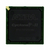
EP2C70F672C8N Altera, EP2C70F672C8N Datasheet - Page 159

EP2C70F672C8N
Manufacturer Part Number
EP2C70F672C8N
Description
IC CYCLONE II FPGA 70K 672-FBGA
Manufacturer
Altera
Series
Cyclone® IIr
Datasheet
1.EP2C5T144C8N.pdf
(168 pages)
Specifications of EP2C70F672C8N
Number Of Logic Elements/cells
68416
Number Of Labs/clbs
4276
Total Ram Bits
1152000
Number Of I /o
422
Voltage - Supply
1.15 V ~ 1.25 V
Mounting Type
Surface Mount
Operating Temperature
0°C ~ 85°C
Package / Case
672-FBGA
No. Of Logic Blocks
4276
Family Type
Cyclone II
No. Of I/o's
422
I/o Supply Voltage
3.3V
Operating Frequency Max
320MHz
Operating Temperature Range
0°C To +85°C
Rohs Compliant
Yes
Family Name
Cyclone® II
Number Of Logic Blocks/elements
68416
# I/os (max)
422
Frequency (max)
402.58MHz
Process Technology
90nm
Operating Supply Voltage (typ)
1.2V
Logic Cells
68416
Ram Bits
1152000
Operating Supply Voltage (min)
1.15V
Operating Supply Voltage (max)
1.25V
Operating Temp Range
0C to 85C
Operating Temperature Classification
Commercial
Mounting
Surface Mount
Pin Count
672
Package Type
FBGA
For Use With
P0304 - DE2-70 CALL FOR ACADEMIC PRICING544-1703 - VIDEO KIT W/CYCLONE II EP2C70N544-1699 - DSP KIT W/CYCLONE II EPS2C70N
Lead Free Status / RoHS Status
Lead free / RoHS Compliant
Number Of Gates
-
Lead Free Status / Rohs Status
Compliant
Other names
544-1688
Available stocks
Company
Part Number
Manufacturer
Quantity
Price
Company:
Part Number:
EP2C70F672C8N
Manufacturer:
ALTERA
Quantity:
1 238
Company:
Part Number:
EP2C70F672C8N
Manufacturer:
ALTERA
Quantity:
7
Part Number:
EP2C70F672C8N
Manufacturer:
ALTERA/阿尔特拉
Quantity:
20 000
Figure 5–10. DCD Measurement Technique for DDIO (Double-Data Rate) Outputs
Altera Corporation
February 2008
clk
INPUT
VCC
When an FPGA PLL generates the internal clock, the PLL output clocks
the IOE block. As the PLL only monitors the positive edge of the reference
clock input and internally re-creates the output clock signal, any DCD
present on the reference clock is filtered out. Therefore, the DCD for a
DDIO output with PLL in the clock path is better than the DCD for a
DDIO output without PLL in the clock path.
Tables 5–55
derivation for different I/O standards on Cyclone II devices. Examples
are also provided that show how to calculate DCD as a percentage.
LVCMOS
LVTTL
2.5-V
1.8-V
1.5-V
SSTL-2 Class I
SSTL-2 Class II
SSTL-18 Class I
HSTL-15 Class I
HSTL-18 Class I
Table 5–55. Maximum DCD for Single Data Outputs (SDR) on Row I/O
Pins
Row I/O Output Standard
Notes
through
(1),
GND
V
CC
(2)
DFF
DFF
5–58
(Part 1 of 2)
D
D
CLRN
CLRN
PRN
PRN
give the maximum DCD in absolution
Q
Q
DC Characteristics and Timing Specifications
145
165
195
120
115
130
Cyclone II Device Handbook, Volume 1
C6
60
65
90
85
1
0
230
255
120
115
130
165
145
155
C7
90
75
230
255
135
175
135
165
205
155
output
C8
90
75
Unit
ps
ps
ps
ps
ps
ps
ps
ps
ps
ps
5–69


