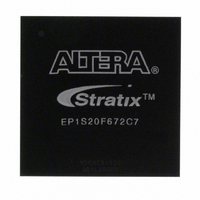
EP1S20F672C7 Altera, EP1S20F672C7 Datasheet - Page 122

EP1S20F672C7
Manufacturer Part Number
EP1S20F672C7
Description
IC STRATIX FPGA 20K LE 672-FBGA
Manufacturer
Altera
Series
Stratix®r
Datasheet
1.EP1S10F780C7.pdf
(276 pages)
Specifications of EP1S20F672C7
Number Of Logic Elements/cells
18460
Number Of Labs/clbs
1846
Total Ram Bits
1669248
Number Of I /o
426
Voltage - Supply
1.425 V ~ 1.575 V
Mounting Type
Surface Mount
Operating Temperature
0°C ~ 85°C
Package / Case
672-FBGA
Family Name
Stratix
Number Of Logic Blocks/elements
18460
# I/os (max)
426
Frequency (max)
420.17MHz
Process Technology
0.13um (CMOS)
Operating Supply Voltage (typ)
1.5V
Logic Cells
18460
Ram Bits
1669248
Operating Supply Voltage (min)
1.425V
Operating Supply Voltage (max)
1.575V
Operating Temp Range
0C to 85C
Operating Temperature Classification
Commercial
Mounting
Surface Mount
Pin Count
672
Package Type
FBGA
Lead Free Status / RoHS Status
Contains lead / RoHS non-compliant
Number Of Gates
-
Lead Free Status / Rohs Status
Not Compliant
Other names
544-1113
Available stocks
Company
Part Number
Manufacturer
Quantity
Price
Company:
Part Number:
EP1S20F672C7
Manufacturer:
SHARP
Quantity:
3 509
Company:
Part Number:
EP1S20F672C7
Manufacturer:
ALTERA
Quantity:
528
Part Number:
EP1S20F672C7
Manufacturer:
ALTERA/阿尔特拉
Quantity:
20 000
Company:
Part Number:
EP1S20F672C7N
Manufacturer:
Harting
Quantity:
1 000
Company:
Part Number:
EP1S20F672C7N
Manufacturer:
ALTERA
Quantity:
3 000
I/O Structure
Figure 2–62. Signal Path through the I/O Block
2–108
Stratix Device Handbook, Volume 1
Interconnect
From Logic
From I/O
To Logic
Array
Array
Row or Column
io_bclk[3..0]
io_boe[3..0]
io_dataout0
io_dataout1
io_bce[3..0]
io_bclr[3..0]
io_cce_out
io_clk[7..0]
io_datain0
io_datain1
io_cce_in
io_cclk
io_coe
io_cclr
Stratix devices have an I/O interconnect similar to the R4 and C4
interconnect to drive high-fanout signals to and from the I/O blocks.
There are 16 signals that drive into the I/O blocks composed of four
output enables io_boe[3..0], four clock enables io_bce[3..0], four
clocks io_bclk[3..0], and four clear signals io_bclr[3..0]. The
pin’s datain signals can drive the IO interconnect, which in turn drives
the logic array or other I/O blocks. In addition, the control and data
signals can be driven from the logic array, providing a slower but more
flexible routing resource. The row or column IOE clocks, io_clk[7..0],
provide a dedicated routing resource for low-skew, high-speed clocks.
I/O clocks are generated from regional, global, or fast regional clocks (see
“PLLs & Clock Networks” on page
signal paths through the I/O block.
Selection
Control
Signal
oe
ce_in
ce_out
aclr/apreset
sclr/spreset
clk_in
clk_out
To Other
IOEs
2–73).
Figure 2–62
IOE
illustrates the
Altera Corporation
July 2005


