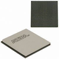
EP1AGX90EF1152I6N Altera, EP1AGX90EF1152I6N Datasheet - Page 63

EP1AGX90EF1152I6N
Manufacturer Part Number
EP1AGX90EF1152I6N
Description
IC ARRIA GX FPGA 90K 1152FBGA
Manufacturer
Altera
Series
Arria GXr
Datasheet
1.EP1AGX20CF484C6N.pdf
(234 pages)
Specifications of EP1AGX90EF1152I6N
Number Of Logic Elements/cells
90220
Number Of Labs/clbs
4511
Total Ram Bits
4477824
Number Of I /o
538
Voltage - Supply
1.15 V ~ 1.25 V
Mounting Type
Surface Mount
Operating Temperature
-40°C ~ 100°C
Package / Case
1152-FBGA
Lead Free Status / RoHS Status
Lead free / RoHS Compliant
Number Of Gates
-
Other names
544-2387
Available stocks
Company
Part Number
Manufacturer
Quantity
Price
- Current page: 63 of 234
- Download datasheet (4Mb)
Chapter 2: Arria GX Architecture
TriMatrix Memory
Figure 2–49. M-RAM Row Unit Interface to Interconnect
© December 2009 Altera Corporation
Direct Link
Interconnects
Table 2–12
and control signal input connections to the row unit interfaces (L0 to L5 and R0 to R5).
Table 2–12. M-RAM Row Interface Unit Signals (Part 1 of 2)
Unit Interface Block
LAB
lists the input and output data signal connections along with the address
L0
L1
L2
L3
C4 Interconnect
M-RAM Block to
LAB Row Interface
Block Interconnect Region
16
datain_a[14..0]
byteena_a[1..0]
datain_a[29..15]
byteena_a[3..2]
datain_a[35..30]
addressa[4..0]
addr_ena_a
clock_a
clocken_a
renwe_a
aclr_a
addressa[15..5]
datain_a[41..36]
Row Interface Block
R4 and R24 Interconnects
Input Signals
Up to 16
Up to 28
M-RAM Block
dataout_a[ ]
datain_a[ ]
addressa[ ]
addr_ena_a
renwe_a
byteena
clocken_a
clock_a
aclr_a
dataout_a[11..0]
dataout_a[23..12]
dataout_a[35..24]
dataout_a[47..36]
A
Arria GX Device Handbook, Volume 1
[ ]
Output Signals
2–57
Related parts for EP1AGX90EF1152I6N
Image
Part Number
Description
Manufacturer
Datasheet
Request
R

Part Number:
Description:
CYCLONE II STARTER KIT EP2C20N
Manufacturer:
Altera
Datasheet:

Part Number:
Description:
CPLD, EP610 Family, ECMOS Process, 300 Gates, 16 Macro Cells, 16 Reg., 16 User I/Os, 5V Supply, 35 Speed Grade, 24DIP
Manufacturer:
Altera Corporation
Datasheet:

Part Number:
Description:
CPLD, EP610 Family, ECMOS Process, 300 Gates, 16 Macro Cells, 16 Reg., 16 User I/Os, 5V Supply, 15 Speed Grade, 24DIP
Manufacturer:
Altera Corporation
Datasheet:

Part Number:
Description:
Manufacturer:
Altera Corporation
Datasheet:

Part Number:
Description:
CPLD, EP610 Family, ECMOS Process, 300 Gates, 16 Macro Cells, 16 Reg., 16 User I/Os, 5V Supply, 30 Speed Grade, 24DIP
Manufacturer:
Altera Corporation
Datasheet:

Part Number:
Description:
High-performance, low-power erasable programmable logic devices with 8 macrocells, 10ns
Manufacturer:
Altera Corporation
Datasheet:

Part Number:
Description:
High-performance, low-power erasable programmable logic devices with 8 macrocells, 7ns
Manufacturer:
Altera Corporation
Datasheet:

Part Number:
Description:
Classic EPLD
Manufacturer:
Altera Corporation
Datasheet:

Part Number:
Description:
High-performance, low-power erasable programmable logic devices with 8 macrocells, 10ns
Manufacturer:
Altera Corporation
Datasheet:

Part Number:
Description:
Manufacturer:
Altera Corporation
Datasheet:

Part Number:
Description:
Manufacturer:
Altera Corporation
Datasheet:

Part Number:
Description:
Manufacturer:
Altera Corporation
Datasheet:

Part Number:
Description:
CPLD, EP610 Family, ECMOS Process, 300 Gates, 16 Macro Cells, 16 Reg., 16 User I/Os, 5V Supply, 25 Speed Grade, 24DIP
Manufacturer:
Altera Corporation
Datasheet:


