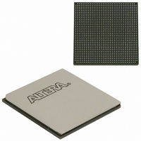
EP2SGX60EF1152C5N Altera, EP2SGX60EF1152C5N Datasheet - Page 131

EP2SGX60EF1152C5N
Manufacturer Part Number
EP2SGX60EF1152C5N
Description
IC STRATIX II GX 60K 1152-FBGA
Manufacturer
Altera
Series
Stratix® II GXr
Datasheet
1.EP2SGX30DF780C5.pdf
(316 pages)
Specifications of EP2SGX60EF1152C5N
Number Of Logic Elements/cells
60440
Number Of Labs/clbs
3022
Total Ram Bits
2544192
Number Of I /o
534
Voltage - Supply
1.15 V ~ 1.25 V
Mounting Type
Surface Mount
Operating Temperature
0°C ~ 85°C
Package / Case
1152-FBGA
Family Name
Stratix II GX
Number Of Logic Blocks/elements
60440
# I/os (max)
534
Frequency (max)
609.76MHz
Process Technology
SRAM
Operating Supply Voltage (typ)
1.2V
Logic Cells
60440
Ram Bits
2544192
Operating Supply Voltage (min)
1.15V
Operating Supply Voltage (max)
1.25V
Operating Temp Range
0C to 85C
Operating Temperature Classification
Commercial
Mounting
Surface Mount
Pin Count
1152
Package Type
FC-FBGA
Lead Free Status / RoHS Status
Lead free / RoHS Compliant
Number Of Gates
-
Lead Free Status / Rohs Status
Compliant
Other names
544-2185
Available stocks
Company
Part Number
Manufacturer
Quantity
Price
Company:
Part Number:
EP2SGX60EF1152C5N
Manufacturer:
ALTERA
Quantity:
533
Part Number:
EP2SGX60EF1152C5N
Manufacturer:
ALTERA/阿尔特拉
Quantity:
20 000
- Current page: 131 of 316
- Download datasheet (2Mb)
Figure 2–86. DQS Phase-Shift Circuitry
Notes to
(1)
(2)
(3)
(4)
Altera Corporation
October 2007
to IOE
DQSn
Pin
Δt
There are up to 18 pairs of DQS and DQSn pins available on the top or the bottom of the Stratix II GX device. There
are up to 10 pairs on the right side and 8 pairs on the left side of the DQS phase-shift circuitry.
The “t” module represents the DQS logic block.
Clock pins CLK[15..12]p feed the phase-shift circuitry on the top of the device and clock pins CLK[7..4]p feed
the phase circuitry on the bottom of the device. You can also use a PLL clock output as a reference clock to the
phaseshift circuitry.
You can only use PLL 5 to feed the DQS phase-shift circuitry on the top of the device and PLL 6 to feed the DQS
phase-shift circuitry on the bottom of the device.
Figure
to IOE
DQS
Pin
Δt
2–86:
to IOE
DQSn
Pin
Δt
A compensated delay element on each DQS pin automatically aligns
input DQS synchronization signals with the data window of their
corresponding DQ data signals. The DQS signals drive a local DQS bus in
the top and bottom I/O banks. This DQS bus is an additional resource to
the I/O clocks and is used to clock DQ input registers with the DQS
signal.
The Stratix II GX device has two phase-shifting reference circuits, one on
the top and one on the bottom of the device. The circuit on the top controls
the compensated delay elements for all DQS pins on the top. The circuit
on the bottom controls the compensated delay elements for all DQS pins
on the bottom.
Each phase-shifting reference circuit is driven by a system reference clock,
which must have the same frequency as the DQS signal. Clock pins
CLK[15..12]p feed the phase circuitry on the top of the device and
clock pins CLK[7..4]p feed the phase circuitry on the bottom of the
device. In addition, PLL clock outputs can also feed the phase-shifting
reference circuits.
control of each DQS delay shift on the top of the device. This same circuit
is duplicated on the bottom of the device.
to IOE
DQS
Pin
Δt
CLK[15..12]p (3)
Notes
Phase-Shift
Circuitry
DQS
(1),
Figure 2–86
(2)
From PLL 5 (4)
to IOE
DQS
Pin
Δt
shows the phase-shift reference circuit
Stratix II GX Device Handbook, Volume 1
DQSn
to IOE
Pin
Δt
Stratix II GX Architecture
to IOE
DQS
Pin
Δt
to IOE
DQSn
Pin
Δt
2–123
DQS Logic
Blocks
Related parts for EP2SGX60EF1152C5N
Image
Part Number
Description
Manufacturer
Datasheet
Request
R

Part Number:
Description:
4. Serial Configuration Devices Epcs1, Epcs4, Epcs16, Epcs64, And Epcs128 Data Sheet
Manufacturer:
Altera Corporation
Datasheet:

Part Number:
Description:
CYCLONE II STARTER KIT EP2C20N
Manufacturer:
Altera
Datasheet:

Part Number:
Description:
CPLD, EP610 Family, ECMOS Process, 300 Gates, 16 Macro Cells, 16 Reg., 16 User I/Os, 5V Supply, 35 Speed Grade, 24DIP
Manufacturer:
Altera Corporation
Datasheet:

Part Number:
Description:
CPLD, EP610 Family, ECMOS Process, 300 Gates, 16 Macro Cells, 16 Reg., 16 User I/Os, 5V Supply, 15 Speed Grade, 24DIP
Manufacturer:
Altera Corporation
Datasheet:

Part Number:
Description:
Manufacturer:
Altera Corporation
Datasheet:

Part Number:
Description:
CPLD, EP610 Family, ECMOS Process, 300 Gates, 16 Macro Cells, 16 Reg., 16 User I/Os, 5V Supply, 30 Speed Grade, 24DIP
Manufacturer:
Altera Corporation
Datasheet:

Part Number:
Description:
High-performance, low-power erasable programmable logic devices with 8 macrocells, 10ns
Manufacturer:
Altera Corporation
Datasheet:

Part Number:
Description:
High-performance, low-power erasable programmable logic devices with 8 macrocells, 7ns
Manufacturer:
Altera Corporation
Datasheet:

Part Number:
Description:
Classic EPLD
Manufacturer:
Altera Corporation
Datasheet:

Part Number:
Description:
High-performance, low-power erasable programmable logic devices with 8 macrocells, 10ns
Manufacturer:
Altera Corporation
Datasheet:

Part Number:
Description:
Manufacturer:
Altera Corporation
Datasheet:

Part Number:
Description:
Manufacturer:
Altera Corporation
Datasheet:

Part Number:
Description:
Manufacturer:
Altera Corporation
Datasheet:


