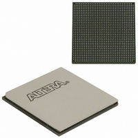
EP2SGX60EF1152C5N Altera, EP2SGX60EF1152C5N Datasheet - Page 148

EP2SGX60EF1152C5N
Manufacturer Part Number
EP2SGX60EF1152C5N
Description
IC STRATIX II GX 60K 1152-FBGA
Manufacturer
Altera
Series
Stratix® II GXr
Datasheet
1.EP2SGX30DF780C5.pdf
(316 pages)
Specifications of EP2SGX60EF1152C5N
Number Of Logic Elements/cells
60440
Number Of Labs/clbs
3022
Total Ram Bits
2544192
Number Of I /o
534
Voltage - Supply
1.15 V ~ 1.25 V
Mounting Type
Surface Mount
Operating Temperature
0°C ~ 85°C
Package / Case
1152-FBGA
Family Name
Stratix II GX
Number Of Logic Blocks/elements
60440
# I/os (max)
534
Frequency (max)
609.76MHz
Process Technology
SRAM
Operating Supply Voltage (typ)
1.2V
Logic Cells
60440
Ram Bits
2544192
Operating Supply Voltage (min)
1.15V
Operating Supply Voltage (max)
1.25V
Operating Temp Range
0C to 85C
Operating Temperature Classification
Commercial
Mounting
Surface Mount
Pin Count
1152
Package Type
FC-FBGA
Lead Free Status / RoHS Status
Lead free / RoHS Compliant
Number Of Gates
-
Lead Free Status / Rohs Status
Compliant
Other names
544-2185
Available stocks
Company
Part Number
Manufacturer
Quantity
Price
Company:
Part Number:
EP2SGX60EF1152C5N
Manufacturer:
ALTERA
Quantity:
533
Part Number:
EP2SGX60EF1152C5N
Manufacturer:
ALTERA/阿尔特拉
Quantity:
20 000
- Current page: 148 of 316
- Download datasheet (2Mb)
High-Speed Differential I/O with DPA Support
Figure 2–89. Stratix II GX Receiver Channel
2–140
Stratix II GX Device Handbook, Volume 1
Up to 1 Gbps
Eight Phase Clocks
+
–
refclk
f
data
Fast
PLL
8
retimed_data
DPA
Figure 2–89
An external pin or global or regional clock can drive the fast PLLs, which
can output up to three clocks: two multiplied high-speed clocks to drive
the SERDES block and/or external pin, and a low-speed clock to drive the
logic array. In addition, eight phase-shifted clocks from the VCO can feed
to the DPA circuitry.
For more information on the fast PLL, see the
Devices
The eight phase-shifted clocks from the fast PLL feed to the DPA block.
The DPA block selects the closest phase to the center of the serial data eye
to sample the incoming data. This allows the source-synchronous
circuitry to capture incoming data correctly regardless of the
channel-to-channel or clock-to-channel skew. The DPA block locks to a
phase closest to the serial data phase. The phase-aligned DPA clock is
used to write the data into the synchronizer.
The synchronizer sits between the DPA block and the data realignment
and SERDES circuitry. Since every channel utilizing the DPA block can
have a different phase selected to sample the data, the synchronizer is
needed to synchronize the data to the high-speed clock domain of the
data realignment and the SERDES circuitry.
DPA_clk
chapter in volume 2 of the Stratix II GX Handbook.
Synchronizer
shows the block diagram of the Stratix II GX receiver channel.
diffioclk
load_en
D
Q
Data Realignment
Circuitry
Dedicated
Interface
Receiver
PLLs in Stratix II GX
Altera Corporation
Data to R4, R24, C4, or
direct link interconnect
Regional or
global clock
October 2007
10
Related parts for EP2SGX60EF1152C5N
Image
Part Number
Description
Manufacturer
Datasheet
Request
R

Part Number:
Description:
4. Serial Configuration Devices Epcs1, Epcs4, Epcs16, Epcs64, And Epcs128 Data Sheet
Manufacturer:
Altera Corporation
Datasheet:

Part Number:
Description:
CYCLONE II STARTER KIT EP2C20N
Manufacturer:
Altera
Datasheet:

Part Number:
Description:
CPLD, EP610 Family, ECMOS Process, 300 Gates, 16 Macro Cells, 16 Reg., 16 User I/Os, 5V Supply, 35 Speed Grade, 24DIP
Manufacturer:
Altera Corporation
Datasheet:

Part Number:
Description:
CPLD, EP610 Family, ECMOS Process, 300 Gates, 16 Macro Cells, 16 Reg., 16 User I/Os, 5V Supply, 15 Speed Grade, 24DIP
Manufacturer:
Altera Corporation
Datasheet:

Part Number:
Description:
Manufacturer:
Altera Corporation
Datasheet:

Part Number:
Description:
CPLD, EP610 Family, ECMOS Process, 300 Gates, 16 Macro Cells, 16 Reg., 16 User I/Os, 5V Supply, 30 Speed Grade, 24DIP
Manufacturer:
Altera Corporation
Datasheet:

Part Number:
Description:
High-performance, low-power erasable programmable logic devices with 8 macrocells, 10ns
Manufacturer:
Altera Corporation
Datasheet:

Part Number:
Description:
High-performance, low-power erasable programmable logic devices with 8 macrocells, 7ns
Manufacturer:
Altera Corporation
Datasheet:

Part Number:
Description:
Classic EPLD
Manufacturer:
Altera Corporation
Datasheet:

Part Number:
Description:
High-performance, low-power erasable programmable logic devices with 8 macrocells, 10ns
Manufacturer:
Altera Corporation
Datasheet:

Part Number:
Description:
Manufacturer:
Altera Corporation
Datasheet:

Part Number:
Description:
Manufacturer:
Altera Corporation
Datasheet:

Part Number:
Description:
Manufacturer:
Altera Corporation
Datasheet:


