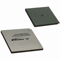
EP2S180F1508C3 Altera, EP2S180F1508C3 Datasheet - Page 108

EP2S180F1508C3
Manufacturer Part Number
EP2S180F1508C3
Description
IC STRATIX II FPGA 180K 1508FBGA
Manufacturer
Altera
Series
Stratix® IIr
Datasheet
1.EP2S15F484I4N.pdf
(238 pages)
Specifications of EP2S180F1508C3
Number Of Logic Elements/cells
179400
Number Of Labs/clbs
8970
Total Ram Bits
9383040
Number Of I /o
1170
Voltage - Supply
1.15 V ~ 1.25 V
Mounting Type
Surface Mount
Operating Temperature
0°C ~ 85°C
Package / Case
1508-FBGA
Family Name
Stratix II
Number Of Logic Blocks/elements
179400
# I/os (max)
1170
Frequency (max)
778.82MHz
Process Technology
90nm (CMOS)
Operating Supply Voltage (typ)
1.2V
Logic Cells
179400
Ram Bits
9383040
Operating Supply Voltage (min)
1.15V
Operating Supply Voltage (max)
1.25V
Operating Temp Range
0C to 85C
Operating Temperature Classification
Commercial
Mounting
Surface Mount
Pin Count
1508
Package Type
FC-FBGA
For Use With
544-1701 - DSP PRO KIT W/SII EP2S180N
Lead Free Status / RoHS Status
Contains lead / RoHS non-compliant
Number Of Gates
-
Lead Free Status / Rohs Status
Not Compliant
Other names
544-2164
Available stocks
Company
Part Number
Manufacturer
Quantity
Price
Company:
Part Number:
EP2S180F1508C3
Manufacturer:
ALTERA
Quantity:
3 000
Company:
Part Number:
EP2S180F1508C3N
Manufacturer:
ALTERA
Quantity:
624
Part Number:
EP2S180F1508C3N
Manufacturer:
ALTERA/阿尔特拉
Quantity:
20 000
High-Speed Differential I/O with DPA Support
Figure 2–58. Stratix II Transmitter Channel
2–100
Stratix II Device Handbook, Volume 1
refclk
Fast
PLL
Dedicated Circuitry with DPA Support
Stratix II devices support source-synchronous interfacing with LVDS or
HyperTransport signaling at up to 1 Gbps. Stratix II devices can transmit
or receive serial channels along with a low-speed or high-speed clock.
The receiving device PLL multiplies the clock by an integer factor W = 1
through 32. For example, a HyperTransport technology application
where the data rate is 1,000 Mbps and the clock rate is 500 MHz would
require that W be set to 2. The SERDES factor J determines the parallel
data width to deserialize from receivers or to serialize for transmitters.
The SERDES factor J can be set to 4, 5, 6, 7, 8, 9, or 10 and does not have to
equal the PLL clock-multiplication W value. A design using the dynamic
phase aligner also supports all of these J factor values. For a J factor of 1,
the Stratix II device bypasses the SERDES block. For a J factor of 2, the
Stratix II device bypasses the SERDES block, and the DDR input and
output registers are used in the IOE.
of the Stratix II transmitter channel.
Each Stratix II receiver channel features a DPA block for phase detection
and selection, a SERDES, a synchronizer, and a data realigner circuit. You
can bypass the dynamic phase aligner without affecting the basic source-
synchronous operation of the channel. In addition, you can dynamically
switch between using the DPA block or bypassing the block via a control
signal from the logic array.
Stratix II receiver channel.
Data from R4, R24, C4, or
direct link interconnect
Interconnect
Local
diffioclk
load_en
10
10
Figure 2–59
Figure 2–58
shows the block diagram of the
Dedicated
Transmitter
Interface
+
–
shows the block diagram
Regional or
global clock
Up to 1 Gbps
Altera Corporation
May 2007


