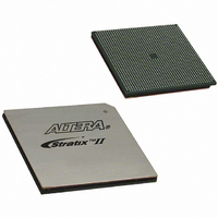
EP2S180F1508C3 Altera, EP2S180F1508C3 Datasheet - Page 13

EP2S180F1508C3
Manufacturer Part Number
EP2S180F1508C3
Description
IC STRATIX II FPGA 180K 1508FBGA
Manufacturer
Altera
Series
Stratix® IIr
Datasheet
1.EP2S15F484I4N.pdf
(238 pages)
Specifications of EP2S180F1508C3
Number Of Logic Elements/cells
179400
Number Of Labs/clbs
8970
Total Ram Bits
9383040
Number Of I /o
1170
Voltage - Supply
1.15 V ~ 1.25 V
Mounting Type
Surface Mount
Operating Temperature
0°C ~ 85°C
Package / Case
1508-FBGA
Family Name
Stratix II
Number Of Logic Blocks/elements
179400
# I/os (max)
1170
Frequency (max)
778.82MHz
Process Technology
90nm (CMOS)
Operating Supply Voltage (typ)
1.2V
Logic Cells
179400
Ram Bits
9383040
Operating Supply Voltage (min)
1.15V
Operating Supply Voltage (max)
1.25V
Operating Temp Range
0C to 85C
Operating Temperature Classification
Commercial
Mounting
Surface Mount
Pin Count
1508
Package Type
FC-FBGA
For Use With
544-1701 - DSP PRO KIT W/SII EP2S180N
Lead Free Status / RoHS Status
Contains lead / RoHS non-compliant
Number Of Gates
-
Lead Free Status / Rohs Status
Not Compliant
Other names
544-2164
Available stocks
Company
Part Number
Manufacturer
Quantity
Price
Company:
Part Number:
EP2S180F1508C3
Manufacturer:
ALTERA
Quantity:
3 000
Company:
Part Number:
EP2S180F1508C3N
Manufacturer:
ALTERA
Quantity:
624
Part Number:
EP2S180F1508C3N
Manufacturer:
ALTERA/阿尔特拉
Quantity:
20 000
Figure 2–3. Direct Link Connection
Altera Corporation
May 2007
block, DSP block, or IOE output
Direct link interconnect from
left LAB, TriMatrix memory
interconnect
Direct link
to left
Interconnect
LAB Control Signals
Each LAB contains dedicated logic for driving control signals to its ALMs.
The control signals include three clocks, three clock enables, two
asynchronous clears, synchronous clear, asynchronous preset/load, and
synchronous load control signals. This gives a maximum of 11 control
signals at a time. Although synchronous load and clear signals are
generally used when implementing counters, they can also be used with
other functions.
Each LAB can use three clocks and three clock enable signals. However,
there can only be up to two unique clocks per LAB, as shown in the LAB
control signal generation circuit in
enable signals are linked. For example, any ALM in a particular LAB
using the labclk1 signal also uses labclkena1. If the LAB uses both
the rising and falling edges of a clock, it also uses two LAB-wide clock
signals. De-asserting the clock enable signal turns off the corresponding
LAB-wide clock.
Each LAB can use two asynchronous clear signals and an asynchronous
load/preset signal. By default, the Quartus II software uses a NOT gate
push-back technique to achieve preset. If you disable the NOT gate
push-up option or assign a given register to power up high using the
Quartus II software, the preset is achieved using the asynchronous load
Local
Figure
Stratix II Device Handbook, Volume 1
ALMs
2–4. Each LAB's clock and clock
Direct link
interconnect
to right
Direct link interconnect from
right LAB, TriMatrix memory
block, DSP block, or IOE output
Stratix II Architecture
2–5


