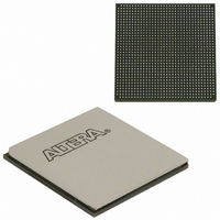
EP2SGX60EF1152I4N Altera, EP2SGX60EF1152I4N Datasheet - Page 15

EP2SGX60EF1152I4N
Manufacturer Part Number
EP2SGX60EF1152I4N
Description
IC STRATIX II GX 60K 1152-FBGA
Manufacturer
Altera
Series
Stratix® II GXr
Datasheet
1.EP2SGX30DF780C5.pdf
(316 pages)
Specifications of EP2SGX60EF1152I4N
Number Of Logic Elements/cells
60440
Number Of Labs/clbs
3022
Total Ram Bits
2544192
Number Of I /o
534
Voltage - Supply
1.15 V ~ 1.25 V
Mounting Type
Surface Mount
Operating Temperature
-40°C ~ 100°C
Package / Case
1152-FBGA
Family Name
Stratix II GX
Number Of Logic Blocks/elements
60440
# I/os (max)
534
Frequency (max)
732.1MHz
Process Technology
SRAM
Operating Supply Voltage (typ)
1.2V
Logic Cells
60440
Ram Bits
2544192
Operating Supply Voltage (min)
1.15V
Operating Supply Voltage (max)
1.25V
Operating Temp Range
-40C to 100C
Operating Temperature Classification
Industrial
Mounting
Surface Mount
Pin Count
1152
Package Type
FC-FBGA
Lead Free Status / RoHS Status
Lead free / RoHS Compliant
Number Of Gates
-
Lead Free Status / Rohs Status
Compliant
Other names
544-2187
Available stocks
Company
Part Number
Manufacturer
Quantity
Price
Company:
Part Number:
EP2SGX60EF1152I4N
Manufacturer:
ALTERA
Quantity:
534
- Current page: 15 of 316
- Download datasheet (2Mb)
Altera Corporation
October 2007
Transmitter Phase Compensation FIFO Buffer
The transmitter phase compensation FIFO buffer resides in the
transceiver block at the PCS/FPGA boundary and cannot be bypassed.
This FIFO buffer compensates for phase differences between the
transmitter PLL clock and the clock from the PLD. After the transmitter
PLL has locked to the frequency and phase of the reference clock, the
transmitter FIFO buffer must be reset to initialize the read and write
pointers. After FIFO pointer initialization, the PLL must remain phase
locked to the reference clock.
Byte Serializer
The FPGA and transceiver block must maintain the same throughput. If
the FPGA interface cannot meet the timing margin to support the
throughput of the transceiver, the byte serializer is used on the
transmitter and the byte deserializer is used on the receiver.
The byte serializer takes words from the FPGA interface and converts
them into smaller words for use in the transceiver. The transmit data path
after the byte serializer is 8, 10, 16, or 20 bits. Refer to
transmitter data with the byte serializer enabled. The byte serializer can
be bypassed when the data width is 8, 10, 16, or 20 bits at the FPGA
interface.
If the byte serializer is disabled, the FPGA transmit data is passed without
data width conversion.
Table 2–3. Transmitter Data with the Byte Serializer Enabled
Input Data Width
16 bits
20 bits
32 bits
40 bits
Stratix II GX Device Handbook, Volume 1
Output Data Width
Stratix II GX Architecture
10 bits
16 bits
20 bits
8 bits
Table 2–3
for the
2–7
Related parts for EP2SGX60EF1152I4N
Image
Part Number
Description
Manufacturer
Datasheet
Request
R

Part Number:
Description:
4. Serial Configuration Devices Epcs1, Epcs4, Epcs16, Epcs64, And Epcs128 Data Sheet
Manufacturer:
Altera Corporation
Datasheet:

Part Number:
Description:
CYCLONE II STARTER KIT EP2C20N
Manufacturer:
Altera
Datasheet:

Part Number:
Description:
CPLD, EP610 Family, ECMOS Process, 300 Gates, 16 Macro Cells, 16 Reg., 16 User I/Os, 5V Supply, 35 Speed Grade, 24DIP
Manufacturer:
Altera Corporation
Datasheet:

Part Number:
Description:
CPLD, EP610 Family, ECMOS Process, 300 Gates, 16 Macro Cells, 16 Reg., 16 User I/Os, 5V Supply, 15 Speed Grade, 24DIP
Manufacturer:
Altera Corporation
Datasheet:

Part Number:
Description:
Manufacturer:
Altera Corporation
Datasheet:

Part Number:
Description:
CPLD, EP610 Family, ECMOS Process, 300 Gates, 16 Macro Cells, 16 Reg., 16 User I/Os, 5V Supply, 30 Speed Grade, 24DIP
Manufacturer:
Altera Corporation
Datasheet:

Part Number:
Description:
High-performance, low-power erasable programmable logic devices with 8 macrocells, 10ns
Manufacturer:
Altera Corporation
Datasheet:

Part Number:
Description:
High-performance, low-power erasable programmable logic devices with 8 macrocells, 7ns
Manufacturer:
Altera Corporation
Datasheet:

Part Number:
Description:
Classic EPLD
Manufacturer:
Altera Corporation
Datasheet:

Part Number:
Description:
High-performance, low-power erasable programmable logic devices with 8 macrocells, 10ns
Manufacturer:
Altera Corporation
Datasheet:

Part Number:
Description:
Manufacturer:
Altera Corporation
Datasheet:

Part Number:
Description:
Manufacturer:
Altera Corporation
Datasheet:

Part Number:
Description:
Manufacturer:
Altera Corporation
Datasheet:


