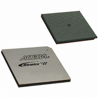
EP2SGX90FF1508C3N Altera, EP2SGX90FF1508C3N Datasheet - Page 20

EP2SGX90FF1508C3N
Manufacturer Part Number
EP2SGX90FF1508C3N
Description
IC STRATIX II GX 90K 1508-FBGA
Manufacturer
Altera
Series
Stratix® II GXr
Datasheet
1.EP2SGX90FF1508C3N.pdf
(314 pages)
Specifications of EP2SGX90FF1508C3N
Number Of Logic Elements/cells
90960
Number Of Labs/clbs
4548
Total Ram Bits
4520448
Number Of I /o
650
Voltage - Supply
1.15 V ~ 1.25 V
Mounting Type
Surface Mount
Operating Temperature
0°C ~ 70°C
Package / Case
1508-FBGA
For Use With
544-1725 - PCIE KIT W/S II GX EP2SGX90N544-1724 - SI KIT W/SII GX EP2SGX90N544-1702 - VIDEO KIT W/SII GX EP2SGX90N
Lead Free Status / RoHS Status
Lead free / RoHS Compliant
Number Of Gates
-
Other names
544-1772
EP2SGX90FF40C3N
EP2SGX90FF40C3NES
EP2SGX90FF40C3N
EP2SGX90FF40C3NES
Available stocks
Company
Part Number
Manufacturer
Quantity
Price
Company:
Part Number:
EP2SGX90FF1508C3N
Manufacturer:
ALTERA30
Quantity:
121
- Current page: 20 of 314
- Download datasheet (4Mb)
Transceivers
2–12
Stratix II GX Device Handbook, Volume 1
f
Refer to the
volume 2 of the Stratix II GX Handbook.
The output buffer, as shown in
high-speed data serializer and consists of a programmable output driver,
a programmable pre-emphasis circuit, a programmable termination, and
a programmable V
Figure 2–8. Output Buffer
Programmable Output Driver
The programmable output driver can be set to drive out differentially
200 to 1,400 mV. The differential output voltage (V
dynamically, or statically set by using the ALT2GXB megafunction or
through I/O pins.
The output driver may be programmed with four different differential
termination values:
■
■
■
■
Serializer
100 Ω
120 Ω
150 Ω
External termination
Output Buffer
Stratix II GX Transceiver Architecture Overview
Programmable
Output
Driver
CM
.
Figure
Programmable
Pre-Emphasis
2–8, is directly driven by the
Programmable
OD
Termination
) can be changed
Altera Corporation
chapter in
October 2007
Output
Pins
Related parts for EP2SGX90FF1508C3N
Image
Part Number
Description
Manufacturer
Datasheet
Request
R

Part Number:
Description:
CYCLONE II STARTER KIT EP2C20N
Manufacturer:
Altera
Datasheet:

Part Number:
Description:
CPLD, EP610 Family, ECMOS Process, 300 Gates, 16 Macro Cells, 16 Reg., 16 User I/Os, 5V Supply, 35 Speed Grade, 24DIP
Manufacturer:
Altera Corporation
Datasheet:

Part Number:
Description:
CPLD, EP610 Family, ECMOS Process, 300 Gates, 16 Macro Cells, 16 Reg., 16 User I/Os, 5V Supply, 15 Speed Grade, 24DIP
Manufacturer:
Altera Corporation
Datasheet:

Part Number:
Description:
Manufacturer:
Altera Corporation
Datasheet:

Part Number:
Description:
CPLD, EP610 Family, ECMOS Process, 300 Gates, 16 Macro Cells, 16 Reg., 16 User I/Os, 5V Supply, 30 Speed Grade, 24DIP
Manufacturer:
Altera Corporation
Datasheet:

Part Number:
Description:
High-performance, low-power erasable programmable logic devices with 8 macrocells, 10ns
Manufacturer:
Altera Corporation
Datasheet:

Part Number:
Description:
High-performance, low-power erasable programmable logic devices with 8 macrocells, 7ns
Manufacturer:
Altera Corporation
Datasheet:

Part Number:
Description:
Classic EPLD
Manufacturer:
Altera Corporation
Datasheet:

Part Number:
Description:
High-performance, low-power erasable programmable logic devices with 8 macrocells, 10ns
Manufacturer:
Altera Corporation
Datasheet:

Part Number:
Description:
Manufacturer:
Altera Corporation
Datasheet:

Part Number:
Description:
Manufacturer:
Altera Corporation
Datasheet:

Part Number:
Description:
Manufacturer:
Altera Corporation
Datasheet:

Part Number:
Description:
CPLD, EP610 Family, ECMOS Process, 300 Gates, 16 Macro Cells, 16 Reg., 16 User I/Os, 5V Supply, 25 Speed Grade, 24DIP
Manufacturer:
Altera Corporation
Datasheet:


