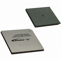
EP2SGX130GF1508I4N Altera, EP2SGX130GF1508I4N Datasheet - Page 36

EP2SGX130GF1508I4N
Manufacturer Part Number
EP2SGX130GF1508I4N
Description
IC STRATIX II GX 130K 1508-FBGA
Manufacturer
Altera
Series
Stratix® II GXr
Datasheet
1.EP2SGX30DF780C5.pdf
(316 pages)
Specifications of EP2SGX130GF1508I4N
Number Of Logic Elements/cells
132540
Number Of Labs/clbs
6627
Total Ram Bits
6747840
Number Of I /o
734
Voltage - Supply
1.15 V ~ 1.25 V
Mounting Type
Surface Mount
Operating Temperature
-40°C ~ 100°C
Package / Case
1508-FBGA
Family Name
Stratix II GX
Number Of Logic Blocks/elements
132540
# I/os (max)
734
Frequency (max)
732.1MHz
Process Technology
SRAM
Operating Supply Voltage (typ)
1.2V
Logic Cells
132540
Ram Bits
6747840
Operating Supply Voltage (min)
1.15V
Operating Supply Voltage (max)
1.25V
Operating Temp Range
-40C to 100C
Operating Temperature Classification
Industrial
Mounting
Surface Mount
Pin Count
1508
Package Type
FC-FBGA
Lead Free Status / RoHS Status
Lead free / RoHS Compliant
Number Of Gates
-
Lead Free Status / Rohs Status
Compliant
Other names
544-2175
Available stocks
Company
Part Number
Manufacturer
Quantity
Price
Company:
Part Number:
EP2SGX130GF1508I4N
Manufacturer:
Sunon
Quantity:
1 000
Part Number:
EP2SGX130GF1508I4N
Manufacturer:
ALTERA/阿尔特拉
Quantity:
20 000
- Current page: 36 of 316
- Download datasheet (2Mb)
Transceivers
Figure 2–23. 20-Bit to 16-Bit Decoding Process
2–28
Stratix II GX Device Handbook, Volume 1
CTRL[1..0]
MSB
19
j
1
h
18
1
15
H
1
17
g
1
G
14
1
16
f
1
13
F
1
15
i
1
13
E
asserted. All 8B/10B control signals, such as disparity error or control
detect, are pipelined with the data in the Stratix II GX receiver block and
are edge aligned with the data.
Figure 2–23
2-bit control indicator.
There are two optional error status ports available in the 8B/10B decoder,
rx_errdetect and rx_disperr. These status signals are aligned with
the code group in which the error occurred.
Receiver State Machine
The receiver state machine operates in Basic, GIGE, PCI Express, and
XAUI modes. In GIGE mode, the receiver state machine replaces invalid
code groups with K30.7. In XAUI mode, the receiver state machine
translates the XAUI PCS code group to the XAUI XGMII code group.
Byte Deserializer
The byte deserializer widens the transceiver data path before the FPGA
interface. This reduces the rate at which the received data needs to be
clocked at in the FPGA logic. The byte deserializer block is available in
both single- and double-width modes.
The byte deserializer converts the one- or two-byte interface into a
two- or four-byte-wide data path from the transceiver to the FPGA logic
(see
deserializer is needed to widen the bus width at the FPGA interface and
1
14
e
1
11
D
Table
1
13
d
1
10
C
Cascaded 8B/10B Conversion
1
2–9). The FPGA interface has a limit of 250 MHz, so the byte
c
12
1
shows how the 20-bit code is decoded to the 16-bit data +
B
9
1
b
11
1
A
8
1
10
a
1
H
7
9
j
G
6
h
8
5
F
g
7
E
4
6
3
D
f
5
2
C
i
1
B
e
4
0
A
d
3
Altera Corporation
Parallel Data
c
2
October 2007
b
1
LSB
a
0
Related parts for EP2SGX130GF1508I4N
Image
Part Number
Description
Manufacturer
Datasheet
Request
R

Part Number:
Description:
CYCLONE II STARTER KIT EP2C20N
Manufacturer:
Altera
Datasheet:

Part Number:
Description:
CPLD, EP610 Family, ECMOS Process, 300 Gates, 16 Macro Cells, 16 Reg., 16 User I/Os, 5V Supply, 35 Speed Grade, 24DIP
Manufacturer:
Altera Corporation
Datasheet:

Part Number:
Description:
CPLD, EP610 Family, ECMOS Process, 300 Gates, 16 Macro Cells, 16 Reg., 16 User I/Os, 5V Supply, 15 Speed Grade, 24DIP
Manufacturer:
Altera Corporation
Datasheet:

Part Number:
Description:
Manufacturer:
Altera Corporation
Datasheet:

Part Number:
Description:
CPLD, EP610 Family, ECMOS Process, 300 Gates, 16 Macro Cells, 16 Reg., 16 User I/Os, 5V Supply, 30 Speed Grade, 24DIP
Manufacturer:
Altera Corporation
Datasheet:

Part Number:
Description:
High-performance, low-power erasable programmable logic devices with 8 macrocells, 10ns
Manufacturer:
Altera Corporation
Datasheet:

Part Number:
Description:
High-performance, low-power erasable programmable logic devices with 8 macrocells, 7ns
Manufacturer:
Altera Corporation
Datasheet:

Part Number:
Description:
Classic EPLD
Manufacturer:
Altera Corporation
Datasheet:

Part Number:
Description:
High-performance, low-power erasable programmable logic devices with 8 macrocells, 10ns
Manufacturer:
Altera Corporation
Datasheet:

Part Number:
Description:
Manufacturer:
Altera Corporation
Datasheet:

Part Number:
Description:
Manufacturer:
Altera Corporation
Datasheet:

Part Number:
Description:
Manufacturer:
Altera Corporation
Datasheet:

Part Number:
Description:
CPLD, EP610 Family, ECMOS Process, 300 Gates, 16 Macro Cells, 16 Reg., 16 User I/Os, 5V Supply, 25 Speed Grade, 24DIP
Manufacturer:
Altera Corporation
Datasheet:


