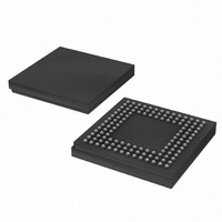
XA3S500E-4CPG132Q Xilinx Inc, XA3S500E-4CPG132Q Datasheet - Page 17

XA3S500E-4CPG132Q
Manufacturer Part Number
XA3S500E-4CPG132Q
Description
IC FPGA SPARTAN-3E 500K 132CSBGA
Manufacturer
Xilinx Inc
Series
Spartan™-3E XAr
Datasheet
1.XA3S100E-4VQG100I.pdf
(37 pages)
Specifications of XA3S500E-4CPG132Q
Number Of Logic Elements/cells
10476
Number Of Labs/clbs
1164
Total Ram Bits
368640
Number Of I /o
92
Number Of Gates
500000
Voltage - Supply
1.14 V ~ 1.26 V
Mounting Type
Surface Mount
Operating Temperature
-40°C ~ 125°C
Package / Case
132-TFBGA, CSPBGA
Package
132CSBGA
Family Name
XA SpartanÂ-3E
Device Logic Units
10476
Device System Gates
500000
Maximum Internal Frequency
572 MHz
Typical Operating Supply Voltage
1.2 V
Maximum Number Of User I/os
92
Ram Bits
368640
Re-programmability Support
Yes
Lead Free Status / RoHS Status
Lead free / RoHS Compliant
Available stocks
Company
Part Number
Manufacturer
Quantity
Price
Company:
Part Number:
XA3S500E-4CPG132Q
Manufacturer:
Xilinx Inc
Quantity:
10 000
Table 16: Propagation Times for the IOB Input Path
Table 17: Input Timing Adjustments by IOSTANDARD
DS635 (v2.0) September 9, 2009
Product Specification
Notes:
1.
2.
Single-Ended Standards
LVTTL
LVCMOS33
LVCMOS25
LVCMOS18
LVCMOS15
LVCMOS12
PCI33_3
HSTL_I_18
HSTL_III_18
SSTL18_I
SSTL2_I
Propagation Times
LVCMOS25 to the Following
Symbol
T
T
Convert Input Time from
IOPLID
The numbers in this table are tested using the methodology presented in
Table 6
This propagation time requires adjustment whenever a signal standard other than LVCMOS25 is assigned to the data Input. When this is
true, add the appropriate Input adjustment from
IOPLI
Signal Standard
(IOSTANDARD)
and
R
The time it takes for data to
travel from the Input pin through
the IFF latch to the I output with
no input delay programmed
The time it takes for data to
travel from the Input pin through
the IFF latch to the I output with
the input delay programmed
Table
9.
Description
Adjustment Below
-4 Speed Grade
Add the
0.43
0.43
0.98
0.63
0.27
0.42
0.12
0.17
0.30
0.15
0
Table
LVCMOS25
IFD_DELAY_VALUE = 0
LVCMOS25
IFD_DELAY_VALUE =
default software setting
17.
Units
Conditions
ns
ns
ns
ns
ns
ns
ns
ns
ns
ns
ns
www.xilinx.com
(2)
(2)
,
,
Table 17: Input Timing Adjustments by IOSTANDARD
Notes:
1.
2.
Differential Standards
LVDS_25
BLVDS_25
MINI_LVDS_25
LVPECL_25
RSDS_25
DIFF_HSTL_I_18
DIFF_HSTL_III_18
DIFF_SSTL18_I
DIFF_SSTL2_I
LVCMOS25 to the Following
Table 19
Convert Input Time from
The numbers in this table are tested using the methodology
presented in
set forth in
These adjustments are used to convert input path times originally
specified for the LVCMOS25 standard to times that correspond to
other signal standards.
Signal Standard
(IOSTANDARD)
and are based on the operating conditions set forth in
DELAY_
VALUE
IFD_
Table
Table 19
0
2
3
2
5
4
6,
Table
and are based on the operating conditions
XA3S100E
XA3S250E
XA3S500E
XA3S1200E
XA3S1600E
Device
9, and
All
Adjustment Below
Table
-4 Speed Grade
Add the
11.
-4 Speed
0.49
0.39
0.49
0.27
0.49
0.49
0.49
0.30
0.32
Grade
Max
2.25
5.97
6.33
6.49
8.15
7.16
Units
ns
ns
ns
ns
ns
ns
Units
ns
ns
ns
ns
ns
ns
ns
ns
ns
17


